Latest Posts
Samsung Electronics Plans AND layoffs
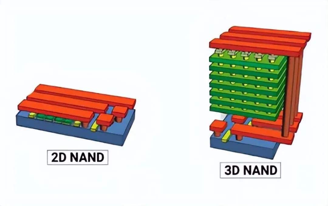
According to industry sources, Samsung Electronics’ latest storage chip development roadmap indicates that the company plans to produce at least 400-layer cell vertical stacking vertical NAND by 2026 to maximize capacity and performance.
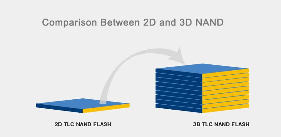
Samsung Electronics plans to adopt a new bonding technology, creating cells and peripheral devices on separate wafers, and then bonding them. This method will achieve “ultra-high” NAND stacks with large storage capacity and excellent heat dissipation performance, which are very suitable for ultra-high capacity SSDs in AI data centers. This chip is called Bonding Vertical NAND Flash, or BV NAND for short, and its bit density per unit area will be increased by 1.6 times.
Samsung Electronics plans to launch V11 NAND by 2027, further developing its stacking technology, with a 50% increase in data input and output speeds. The goal is to develop NAND chips with more than 1,000 layers by 2030 to achieve higher density and storage capacity.
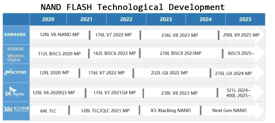
SK Hynix has also begun the development of 400-layer NAND Flash and is currently developing process technologies and equipment, with the goal of achieving mass production by the end of next year and full-scale mass production by the first half of 2026.
Kioxia has indicated in its technology roadmap that the number of 3D NAND layers will grow at an annual rate of 1.33 times, reaching a level of 1,000 layers by 2027, with NAND chip density reaching 100 Gbit/mm²
This year, as the NAND processes of storage manufacturers have been iterated, the supply of NAND with more than 200 layers has increased, and high-density NAND has gradually made progress in market applications:
Samsung’s 236-layer V8 TLC NAND production has increased significantly, and 290-layer V9 TLC/QLC NAND has begun mass production;
SK Hynix has expanded the application of 238-layer NAND in enterprise-level SSDs and launched 321-layer NAND Flash;
Kioxia and Western Digital have promoted the acceleration of 218-layer BiCS8 NAND in OEM manufacturers, and 2Tb QLC NAND produced using BiCS8 and CMOS bonding technology has begun sampling;
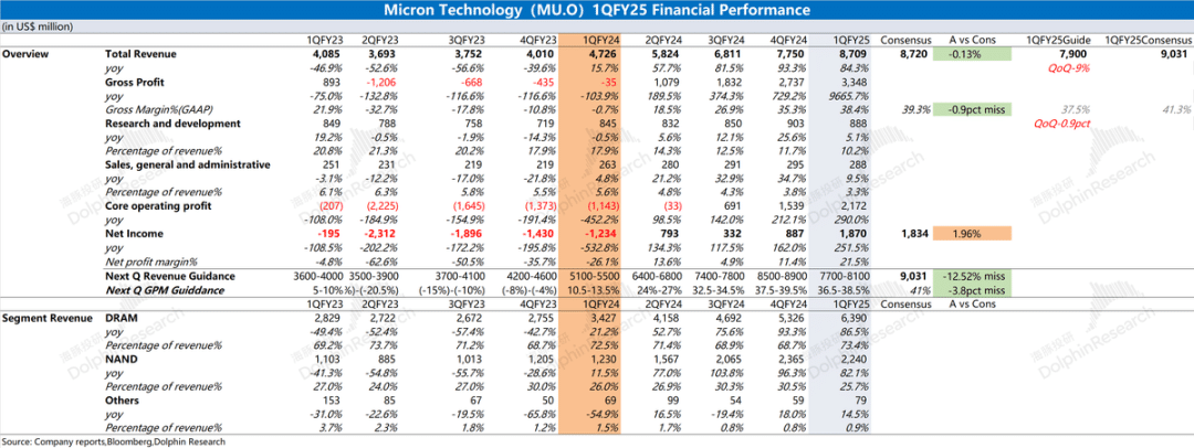
Micron has mass-produced 276-layer G9 TLC NAND and has adopted it in SSDs for client-side OEMs.
Samsung Electronics undergoes four rounds of massive layoffs
Samsung Electronics to Implement Four Rounds of Voluntary Retirement, Contract Manufacturing Team to be Reduced by Over 30%.
According to a high-ranking official at Samsung Electronics on November 2nd, the first round of voluntary retirement will be offered to CL3 (Associate Manager level) employees who have worked for more than 15 years but have not received a rank in the last 5 years. The second round will be for employees who have worked continuously for over 10 years; if the target is not met, the third round will be expanded to all employees. It is reported that the final fourth round will be conducted as part of normal operations. The conditions for voluntary retirement are expected to include a compensation package totaling approximately 400 million won (currently about 2.064 million yuan), which includes a severance payment based on CL3 and four months’ salary of 380 million won.
Especially, the 8-inch contract manufacturing and technology team will see a reduction of over 30%. It is understood that Samsung is considering a proposal for voluntary retirement for unpaid employees. This comes after Samsung Electronics recorded a profit shock in the third quarter of this year due to a decline in competitiveness in its flagship semiconductor business, triggering a crisis theory within the group.
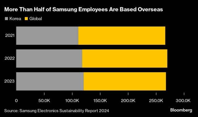
This is interpreted as part of a reform plan to overcome aging business environments and poor performance.
Samsung recently announced third-quarter revenue of 79.1 trillion won, slightly exceeding the expected 79 trillion won, and operating profit of 9.18 trillion won, which exceeded the expected 9.1 trillion won, but was significantly lower than the estimated 11.456 trillion won in operating profit by the London Stock Exchange. Samsung’s Vice Chairman and newly appointed head of the Device Solutions (DS) division, Jeon Yong-hyun, apologized rarely after releasing the performance guidance.
Among them, Samsung’s semiconductor division announced an operating profit of 3.86 trillion won (about 2.8 billion USD) for the third quarter, a 40% decrease from the previous quarter.
Although its memory chip division benefited from strong demand for artificial intelligence (AI) and traditional server products, Samsung stated that “inventory adjustments had a negative impact on mobile demand.” The company said it is also dealing with the issue of “increased supply of mature process products from China.”
Additionally, according to insiders on November 1st, Samsung Electronics has shut down over 30% of the 4nm, 5nm, and 7nm wafer contract manufacturing production lines at its Pyeongtaek 2 (P2) and 3 (P3) factories, and plans to expand the suspension of production to about 50% by the end of the year. The company intends to gradually halt production while monitoring customer orders.





Leave a comment