The changes in the semiconductor industry in 2024 are greater than the sum of the changes over the previous five years combined.
In 1995, Nvidia’s first chip, the NV1, faced numerous setbacks, leaving the company with only 30 days of working capital. By 2024, Nvidia’s Blackwell GPU was in such high demand that the company’s market value had surpassed $3.6 trillion. Also in 1995, Intel held over 75% of the global PC processor market, establishing its leadership in the personal computer market. Fast forward to 2024, Intel’s stock price has plummeted nearly 60% since the beginning of the year, with its market value dropping to over $80 billion, marking the first time in three decades that it has fallen below the $100 billion threshold. The changes in the market values of these two semiconductor giants are a microcosm of the current semiconductor landscape.There is a saying that goes, “People tend to overestimate the changes that happen in a year, but underestimate the changes that happen in five years.” Looking back, the changes in the semiconductor industry in 2024 have been greater than the sum of the changes over the previous five years. 2024 will be a turning point for the semiconductor industry. Why do we say that? Because, as an industry, the semiconductor sector is inseparable from the basic characteristics that define it: division of labor, products, and services. And products like computers and chips cannot be separated from the science behind them. The industry and science are interdependent, and even before the 1970s, the industry was clearly dependent on science. (The controversy over the Silliman affair was a watershed in the relationship between science and industry.) The significant changes in the semiconductor industry this year are the result of a three-way tug-of-war between technology (science), policy, and the market.
01 The Transformation of Semiconductor Companies
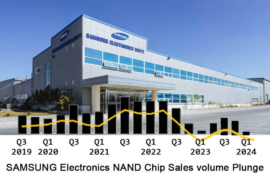
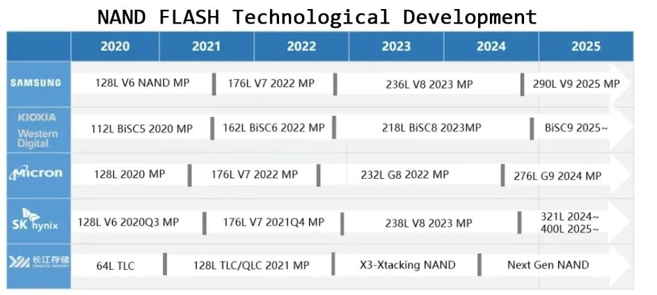
In 2024, there have been many news items that have stimulated the nerves of industry insiders. The most prominent is still the surging market value of Nvidia. Microsoft and Apple have been the two companies with the highest market value in the world since 2010. Although the two have been “entangled” in the ranking of “U.S. stock market leader” for more than 10 years, no one else has replaced them. On June 18, 2024, local time, Nvidia’s stock price rose by 3.51%, closing at $135.58, with a total market value of $3.335 trillion, surpassing both Microsoft and Apple to become the company with the highest market value in the world. This is a change that affects the whole world, such as in August 2011 when Apple first defeated ExxonMobil to win the title of the world’s most valuable company, which was also a symbolic moment for technology companies to defeat traditional oil companies. And Nvidia becoming the world’s most valuable company represents a shift in the focus of technology industry development. Traditional fields represented by Apple, such as consumer electronics and software, have led an era in the past, while Nvidia’s first place means that the focus of technology industry development is accelerating towards the AI field. In addition, on November 8th of this year, Nvidia replaced Intel as a component of the Dow Jones Industrial Average. S&P Global stated that the adjustment of components is to ensure that the index has a more representative semiconductor exposure. In fact, this is also proof: AI has truly entered the commercial track, and the impact of AI on the semiconductor industry is growing. In the semiconductor industry in 2024, in addition to the continuously increasing upper limits, there are also constantly refreshed lower limits. There are two giants in the semiconductor industry, which are well-known to everyone: Intel and Samsung. Since 1992, Intel has been the world’s largest semiconductor manufacturer and has been leading for 25 years. Although Samsung’s chip business surpassed Intel for the first time in 2017, it is still a constant struggle for the leading position. This year’s two chip giants seem to be stuck in a “swamp,” constantly struggling. As mentioned earlier, Intel’s market value has fallen due to its continuously losing performance. In the second quarter of this year, Intel’s loss reached $1.6 billion, far higher than the loss of $437 million in the previous quarter. And the latest third-quarter financial report announced its largest quarterly loss in its 56-year history – $16.6 billion (about 118.2 billion yuan). Samsung is also in a difficult situation in 2024. In October, Samsung announced that its third-quarter operating profit was about 91 trillion won, lower than the market expectation of 115 trillion won. Jeon Young-hyun, head of Samsung’s electronic device solutions department, also issued an apology, stating that the company’s performance did not meet market expectations, causing people’s worries about the company’s basic technical competitiveness and the future. As the senior management leading the company’s operations, they will take responsibility. (It seems that South Korea has also learned the apology system from Japan.) Similarly, the stock market reflects the company’s situation. Samsung’s stock price fell to 51,700 won on November 14th, local time, a record low since June 24, 2020. If this trend continues, Samsung’s stock price for the whole year will be the worst performance in over 20 years.
02 Europe’s “Decadence”
The changes in 2024 are not only the obvious corporate rankings but also regional changes. Amid global government attention to the semiconductor industry, there is a region where semiconductors have been declining throughout the year – Europe. Many people may not have noticed, but the data from WSTS cannot be deceived.
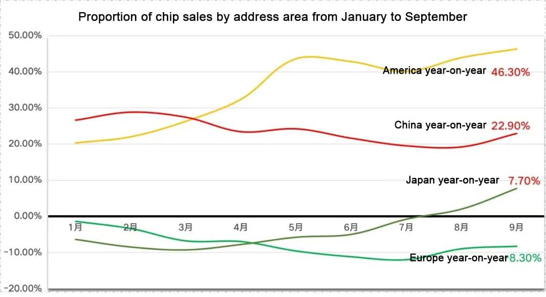
We have calculated the chip sales announced by WSTS since January of this year, and so far, the chip sales in Europe for the whole year have been negative year-on-year. Of course, there is also Japan, but Japan’s year-on-year growth has slightly turned positive in August and September. The European semiconductor industry fell into a weak state in 2024. The “three giants” of the European semiconductor industry: Infineon, STMicroelectronics, and NXP, all have poor revenue. Infineon’s revenue in the third quarter reached 3.702 billion euros, a year-on-year decrease of 9%. Currently, Infineon has lowered its performance outlook for 2024, adjusting this year’s revenue expectation to 15.5 billion to 16.5 billion euros, lower than the previous expectation of 16.5 billion to 17.5 billion euros. STMicroelectronics’ net revenue in the third quarter was 3.25 billion US dollars, a year-on-year decrease of 26.6%. NXP’s revenue decreased by 5.4% to 3.25 billion US dollars, slightly lower than the analysts’ expected 3.26 billion US dollars. Nowadays, Europe’s automotive and industrial markets have already shown negative growth.
From a more specific level of observation, the performance of optoelectronics and discrete devices is not satisfactory, the MCU market shows a shrinking trend and has shown negative growth, and the analog market has also experienced a long period of decline.
03 Tracing Back to the Source
The only constant in the world is change itself. This year, there have been so many changes in the semiconductor industry. Let’s trace back to the root causes and examine policies, markets, and technology.
| Revenue of the 2024 top 10 global semiconductor companies | ||||
| 2023 ranking | 2024Q3 ranking | Company | Q3 revenue in 2024 | Year-on-year revenue |
| 5 | 1↑ | NVIDIA | 300.4(Q2) | 122.40% |
| 6 | 2↑ | SKHynix | 116.75(Q2) | 124.79% |
| 9 | 3↑ | APPLE | 857.77 | 4.87% |
| 2 | 4↓ | Samsung | 560 | 7.35% |
| 1 | 5↓ | Intel | 132.84 | -6.17% |
| 4 | 6↓ | Broadcom | 130.72 | 47.27% |
| 3 | 7↓ | Qualcomm | 93.9 | 8.77% |
| 7 | 8↓ | AMD | 68.19 | 17.57% |
| 10 | 9↑ | Texas Instruments | 41.51 | -8.41% |
| 8 | 10↓ | STMicroelectronics | 32.51 | -26.63% |
| Source: Financial Report Semiconductor Industry Vertical and Horizontal Tabulation | ||||
The impact of policies on the industry is self-evident. At the policy level, the United States, Europe, Japan, South Korea, and Vietnam have all released semiconductor-related policies in the past two years. However, looking at the current situation, the implementation of the semiconductor policies in the United States and Europe has not been significant.
So far, more than half of the $52 billion subsidy in the U.S. Chip Act has been allocated, with over $35 billion granted to about 26 projects. Yet, the funds seem to be slow in coming, with Intel constantly complaining, “It’s been two years, and we haven’t seen a penny.”
Policy
The U.S. Chip Act is even more precarious after Trump’s potential return to office next year, as he is known to be opposed to the act. In interviews, Trump has bluntly stated, “It’s terrible.” The European Chip Act has not made any waves either. Proposed in 2022, there are not many factories being built in Europe, and Intel’s project has not even started. However, it is important to note that the Chip Act has played a role in attracting investment without actual capital. Companies like Intel, TSMC, Samsung, Micron, GlobalFoundries, and Amkor have already begun constructing factories in various regions of the United States due to the subsidies from the Chip Act. Even if the timeline for financial assistance is extended or the subsidies are canceled, it is unlikely that the partially constructed fabs will become abandoned projects. It can be said that for semiconductor companies, building factories in the United States is already an inevitable action. Although the Chip Act has not been fully implemented and Trump denies its effectiveness, there is no doubt that he supports the repatriation of advanced manufacturing to the United States. This is why, when looking at Intel, we also believe that Intel will not be as bad as it seems. Despite Intel being constantly criticized, we cannot ignore its significant role on the geopolitical stage and as one of the U.S. government’s chips in the semiconductor industry and foreign policy strategies. When considering Intel’s prospects, we must not overlook the elements of U.S. strategy and geopolitics. The semiconductor industry now occupies an important strategic position, which is common knowledge. Regardless of whether it can reach the extreme 3nm process, globally, there are only three companies capable of manufacturing advanced process chips: TSMC, Intel, and Samsung. A significant part of the U.S. Chip Act’s plan is directed towards Intel’s construction of two large factories in Arizona and the building of two more factories in Ohio. Therefore, Intel’s future is still full of Highlights. It is not appropriate to directly assume that it will “decline to the end.”
Market
Why has the term “involution” started to be used domestically in recent years? It is because the pace of technological innovation has slowed down, and with the impact of the three-year pandemic, China’s economic development speed has also slowed down under various pressures, leading to “involution.” The “second curve” theory believes that industrial development has a life cycle, and any growth curve is a parabola that rises and then falls. The secret to sustained growth is to start a new growth curve before the inflection point appears, thus forming a continuous improvement and development trend with the new and old momentum in sequence. We are now in the depression period of the last round of technological and industrial revolutions. To make the economy prosperous again, a new round of technological and industrial revolutions must be ignited.This is the inflection point brought by the cycle. The new round of explosion is undoubtedly in AI, which is also a consensus among many industry insiders.
Tech
AI brings new growth points to the market, with many technologies hidden under AI. Above AI, we need to see the development of technology. The outbreak of AI this time is undoubtedly driven by technology. The emergence of GenAI has been brewing for a long time. And this outbreak of AI has driven other technologies that were brewing. The first representative is: TSMC’s advanced packaging process, CoWoS. The two most concerned products in the semiconductor industry: GPU, HBM, both of these products rely on advanced processes to be produced. And TSMC’s CoWoS packaging plays a very key role, so that some people have begun to jokingly call “TSMC will be the world’s first packaging and testing factory.” Here, the packaging and testing, which originally belonged to the back-end process, has shown a clear trend of front-end. And in the process of HBM suppliers continuously improving the stacking density, the interconnection between the fifth-generation HBM (i.e., HBM4) and the logic layer in the future will be jointly completed by storage giants and foundries. According to SK Hynix, HBM4 will greatly change the industry’s perception of DRAM as a “universal chip,” turning it into a customized storage special process chip. In this process, the related technical know-how will be jointly undertaken by foundries and storage factories, which is also the meaning of TSMC’s “Foundry 2.0” plan this year. The second representative is: the architecture competition, that is, the market competition between x86 and Arm, RISC-V. This year, it is obvious that the market share of Arm architecture chips is increasing. The x86 alliance has made it very clear not long ago: face to face. Although it seems to be a change in the market among the three architectures at first glance, it is actually a thirty-year-long competition between CISC (Complex Instruction Set) and RISC (Reduced Instruction Set), these two chip design philosophies. This competition is essentially an extension of the development of computer architecture as a “science and technology” in the “industry” field. The emergence of AI has given these two design philosophies more application scenarios. From the current point of view, the architecture under the RISC architecture (Arm, RISC-V) indeed has an innate advantage because it has the low power consumption and high energy efficiency that AI naturally needs. This also means that Arm may one day achieve a higher market share, which is driven by both technology and the market.

