Latest Posts
What is NAND Flash Memory and How it works
What is Flash memory
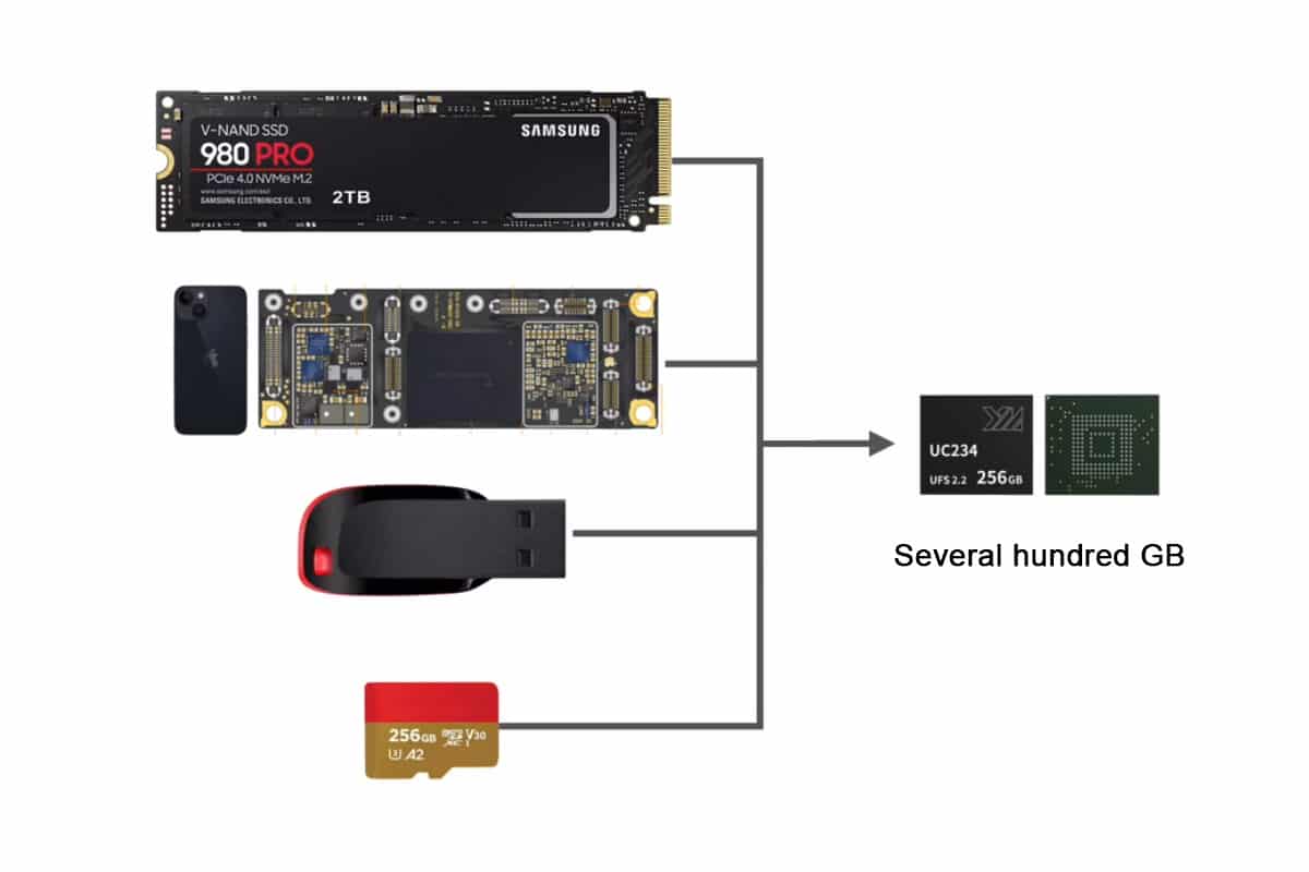
Flash memory is the core of storage for solid-state drives, USB drives, and memory cards. It can typically store hundreds of gigabytes of data in a space the size of a fingernail. It is an invention that is as renowned as the Nobel Prize. Flash memory storage relies on floating-gate MOSFETs. Before discussing floating-gate transistors, let’s briefly introduce MOSFETs, as floating-gate transistors are an improvement based on MOSFETs. The principle of MOSFETs is quite understandable. These three black areas are metal conductors, and the n-type semiconductors on both sides contain many free electrons. If we apply electricity to the n-type semiconductors, they can conduct, acting like a piece of wire. The p-type semiconductor in the middle has very few free electrons, so when we apply voltage to the base, it is cut off because the concentration of free electrons in the p-region is too low to form a conductive channel.
To make the MOSFET conduct, we can apply a voltage to its gate, attracting the electrons in the p-region towards the gate.
Because there is a layer of silicon dioxide between the gate and the p-region, which is insulating, free electrons cannot pass through under normal circumstances. So, when we apply voltage to the gate, the free electrons in the p-region gather near the insulating layer, forming a conductive channel, and thus it conducts.
Floating-gate mosfets
However, when we remove the gate voltage, the electrons gathered near the insulating layer disperse, and no conductive channel is formed. Since no current flows, the MOSFET is cut off at this time. This is the circuit symbol for a MOSFET. Simply put, when we apply a high voltage to its gate, it will conduct, and when we apply a low voltage, it will be cut off.
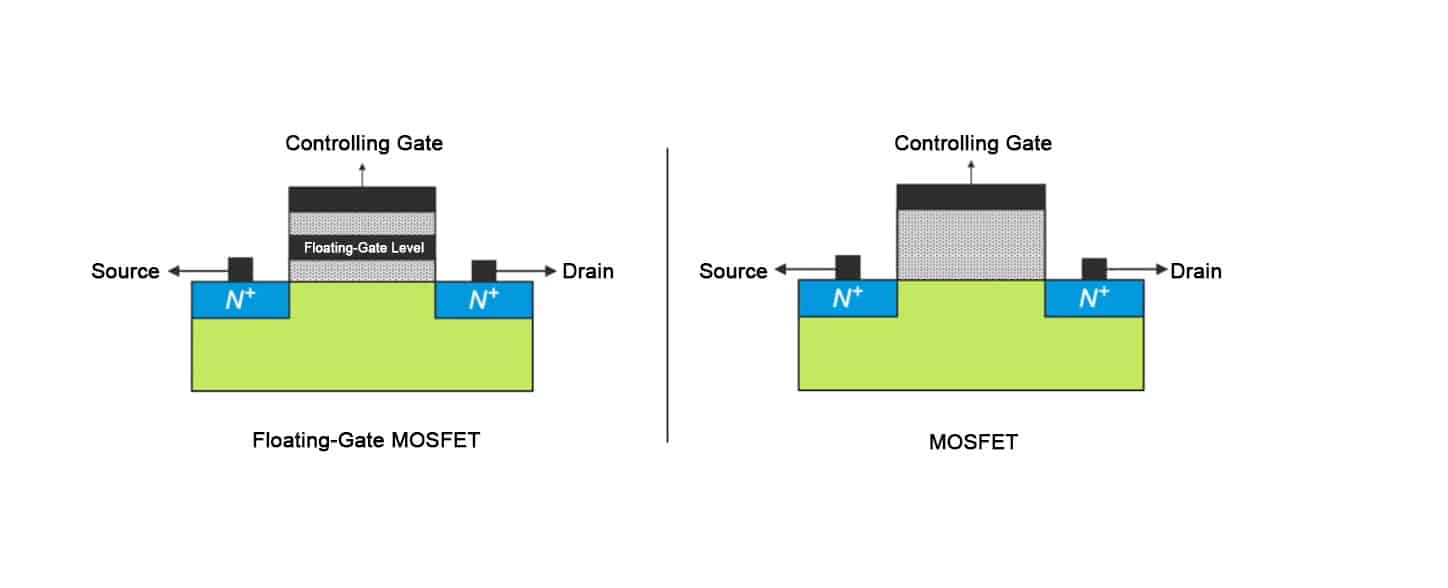
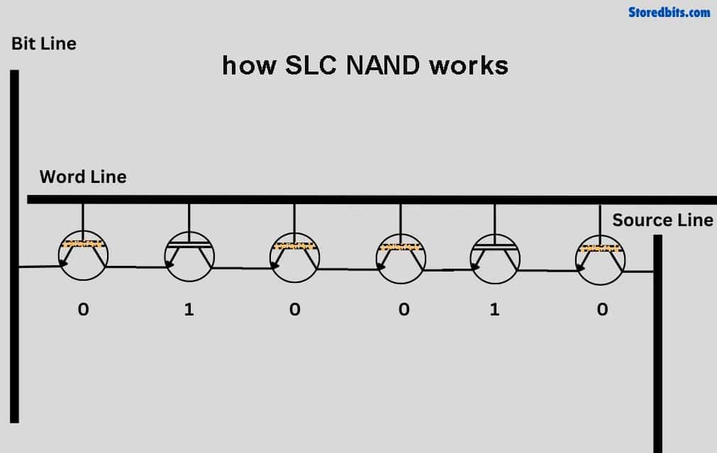
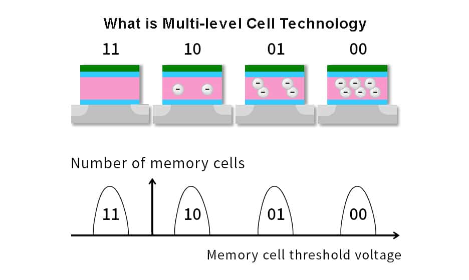
Floating-gate MOSFETs are very similar to MOSFETs, except for an additional bar in the middle, which represents the floating gate. Since they are both MOSFETs, their structures are similar. A floating-gate MOSFET has an additional conductive floating gate layer added to the oxide layer of a MOSFET, allowing it to store information. Let’s talk about how to write information first. If we apply a high voltage of 20 volts to the gate and 0 volts to the substrate, some of the free electrons in the channel will be attracted to the floating gate layer. Even if we then power off, the free electrons will still be stored in the floating gate layer because the floating gate layer is insulated by silicon dioxide layers above and below, and the free electrons simply cannot escape. This is how information is stored, with the charge stored being considered a logical zero.There is also a question about how electrons can pass through the tunnel oxide layer, which is also an insulating layer. This is actually due to the tunneling effect. For example, a silicon dioxide oxide layer is normally insulating, but if we apply a voltage large enough, greater than 10 million volts per centimeter, electrons can pass through this insulating layer. This is the tunneling effect. When we apply a 20V high voltage to the gate, due to the thinness of the tunnel layer and the high voltage per unit thickness it withstands, electrons from the p-region are attracted. It is important to note that at this time, do not apply voltage to the drain, or a sub-threshold conduction channel will form, and electrons will flow in this manner, which would hinder the occurrence of the tunneling effect.
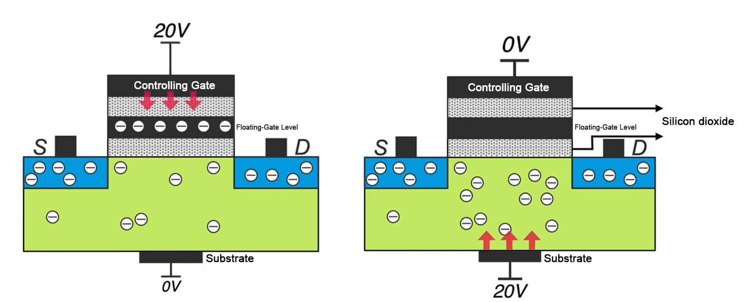
When we apply a low voltage of 10 volts, electrons cannot pass through the insulating layer, just like a conventional MOSFET. Understanding the principle of flash memory writing makes it easy to understand its parameter principle. We just need to apply a high voltage of 20 volts to its substrate while applying 0V to the gate. At this time, the free electrons imprisoned in the floating gate layer will be attracted out, and the data will be erased. Erasing is writing a logical one. Storing one bit of information requires only one floating-gate MOSFET. To store 1GB of information, at least 8.5 billion floating-gate transistors are needed. How do we control so much information?
How does nand flash work
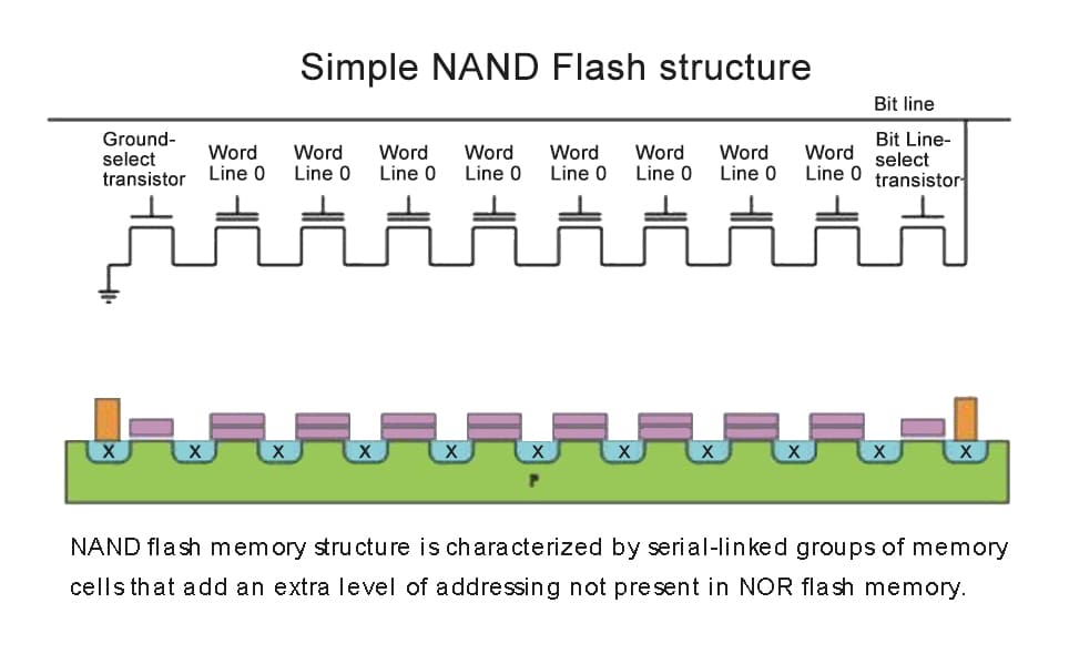
You can see this is a flash memory block that can store 16 bits of information. The middle ones are floating-gate MOSFETs that store information. The top and bottom ones are conventional MOSFETs that play a controlling role here. The horizontal ones are its word lines, connecting the gates of these rows of MOSFETs. The vertical ones are its bit lines. Its writing minimum unit is a page. A page is a row. When we want to write, we first need to erase all the data in this entire block, which means releasing the electrons stored in the floating gate layer, and all storage units will become logical ones.

How do we write by page? For example, if we want to write the page “word1,” we need to apply 20 volts of high voltage to the radiation MOSFETs of this page, and other MOSFETs should not be given high voltage. In this way, only the data of this page with 20 volts of high voltage can possibly be written. If we want to store a charge and write 0, we write 0 to its corresponding bit line, so free electrons will be attracted to the floating gate layer, and this bit will be written as logical 0. If we want to write 1, it’s very simple because we need to erase before writing, and after erasing, the data is all 1. We just need to keep the data unchanged. For example, if we want to write 1 to this bit, we write a high voltage to its bit line, which will hinder the tunneling effect. So, free electrons will not be captured by the floating gate layer, and it will remain logical one unchanged. The minimum unit for writing data is a page of data, and the minimum unit for erasing data is to erase the entire block. We need to give all of them zero volts and then apply a high voltage of 20 volts to the substrate.
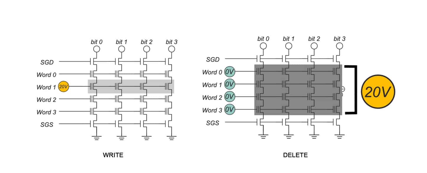
You might be curious why the minimum unit for erasing is an entire block of data. Look at its cross-section, and you will understand. All storage units of this flash memory share a substrate. Just by applying a high voltage of 20 volts to the substrate, the operation of erasing the entire block of data can be completed. The minimum writing unit is a page because the gates of the MOSFETs on this page are connected together. This block of data can store 16 bits of data. One page is 4 bits of data, and a real flash memory page has 65,536 storage units per block. There are 512 pages in the data, so a block of flash memory data can store more than 33 million data points. This is what we call 4MB of data. Even if we want to write one bit of data, we also have to erase these more than 33 million bits of data before we can write.A block of data is 4MB, and to make up 1GB, you would need 256 flash memory blocks. The packaging size of the chip is standardized. To package enough storage units within the chip, the storage units must be made small enough to fit more of them in. However, as they are downsized, many issues arise. For instance, the tunnel oxide layer also becomes thinner. Due to the process of erasing and writing, electrons need to pass through the oxide layer repeatedly. If this happens too many times, the tunnel oxide layer can become damaged and fail to block the electrons, leading to data not being well preserved.
What is 3d nand flash

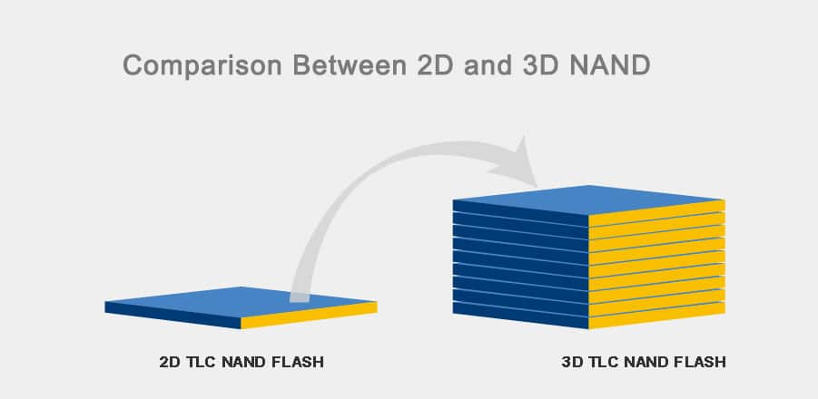
To address this issue, humans invented 3D NAND flash, which eliminates the need to increase the number of storage units by downsizing MOSFETs. This is a 4-layer flash that stands the conductive channels upright, with horizontal pages of data. This area represents a block of data, and the middle contains all its storage units. So far, 3D NAND flash memory has achieved a stack of 232 layers, with a storage density of about 15GB per square millimeter. By using 3D stacking, not only can the unit capacity be increased several times, but also, because of the three-dimensional technology, the size of the storage units does not need to be reduced. As a result, the number of write-erase cycles is increased by more than tenfold. This is my understanding of flash memory technology, and I hope it helps your comprehension.



Leave a comment