Latest Posts
what does nm mean in flash chips?
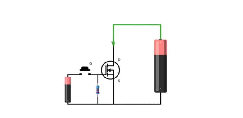
In today’s mainstream CPUs or NAND Flash, there are often hundreds of billions of transistors packaged inside. What exactly are these transistors? And what is their construction like? Broadly speaking, transistors are mainly divided into two types: BJT bipolar junction transistors and FET field-effect transistors. Currently, most of the transistors packaged in chips are MOSFETs, which are a type of field-effect transistor. This is its circuit symbol.When we apply a high voltage to its gate, the drain and source can conduct, but when we apply a low voltage, it will cut off, which is equivalent to being disconnected.
Next, let’s look at its construction. This is an early planar transistor, mainly used for chip processes ranging from 10,000 nanometers to 22 nanometers. Now, let’s talk about how it works. These are its drain and source, which are essentially two pieces of n-type semiconductors with a high concentration of free electrons. In the middle is the substrate, which is essentially a p-type semiconductor with a low concentration of free electrons. If we connect the drain and source with electricity at this time, it cannot conduct.Because although the p-type substrate has a certain amount of electrons, the concentration is extremely low and far from enough to build an effective electrical conduction path between the source and drain. At this time, people added an insulating layer on the substrate, and then added a highly conductive metal plate on the substrate as the gate. In this way, when we apply voltage to the gate, the electrons in the p-type substrate will be attracted to the vicinity of the insulator, and the concentration of free electrons at the junction of the substrate and the insulator will become higher. At this time, when we connect the source and drain with electricity again, it will conduct. Because an effective electrical conduction path has been built between the source and drain.
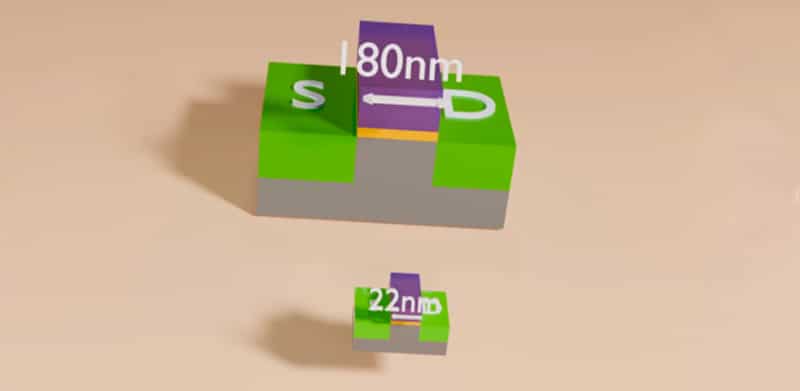
For this planar transistor, the chip process refers to the length of its gate. For example, if its gate length is 180 nanometers, then it is a chip with a 180-nanometer process. However, when the chip process is reduced to 22 nanometers and below, due to the short-channel effect, the distance between the drain and the source is too short, and the drain electric field will interfere with the gate’s control over the channel, leading to an increase in leakage current. This invisibly increases power consumption, and the channel is difficult to shorten further.
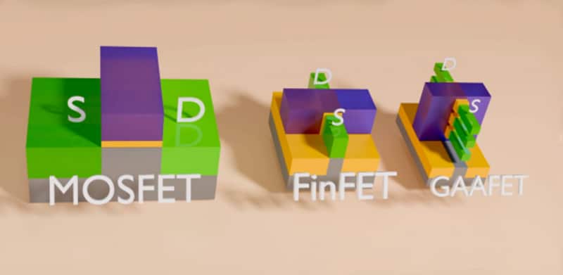
Therefore, when entering the era of three-dimensional transistors, such as FinFET and GAAAFET transistors, the “nanometers” in chip manufacturing no longer refer to the gate length of the transistor. The term “nanometers” is more of a marketing term. For example, in a 3-nanometer process chip, the gate length of its transistors may be between 15 and 20 nanometers. You can see the difference in construction between them and conventional MOSFETs. The conventional construction direction is horizontal, while the construction direction of three-dimensional transistors is vertical. Next, let’s look at the construction of FinFET and GAAAFET transistors. First, let’s talk about FinFET. The FinFET transistor was invented by Professor Hu Shengming from Taiwan Province and is mainly used in the 22-3 nanometer process nodes. Because its channel is protruding and looks like a fish fin, it is called a fin transistor. This type of transistor has solved the short-channel effect well, but it is still essentially a MOSFET. The working principle of the fin transistor is similar to that of the planar transistor. The bottom is a large substrate, which is a p-type semiconductor. Its two sides are covered with two insulators, and above are two N-type semiconductors as the source and drain. Then, the three sides are surrounded by insulators, and the top is a highly conductive metal as the gate. When we electrify the gate, all three sides of the p-type substrate will be attracted by the electric field, providing better gate control.

Despite the improved gate control provided by three-dimensional structures, for extremely small sizes, such as below three nanometers, electric field interference and leakage current are still hard to avoid. Therefore, the ingenious humans invented the GAAAFET transistor, also known as the gate-all-around transistor, which is mainly used below three nanometers. You can take a look at its structure: the bottom layer is the substrate, followed by two layers of oxide, which can be seen as the tray of the transistor. Above that are three very thin nano channels, composed of n-type and p-type semiconductors. Then, a layer of oxide (insulating material) is wrapped around the four sides of its p-area, and a piece of highly conductive metal is added as the gate. Compared to the three-sided gate of FinFET, GAAAFET achieves a 360-degree gate wrap, hence the name gate-all-around transistor. This further strengthens the gate control capability, and these three channels essentially belong to one transistor. Devices like Central Processing Units (CPUs) and Graphics Processing Units (GPUs) often need to handle large amounts of data and complex computational tasks, which requires the transistors that make them up to have a strong current driving capability for rapid signal transmission and processing.

GAAFET transistors, due to their multi-channel design, can significantly enhance the driving capability of the transistor. Without significantly reducing the gate length, FinFET and GAAAFET transistors increase gate control by wrapping around the gate from multiple angles, reducing the unit area occupied by the transistor. This allows for more transistors to be integrated within the same area, effectively shortening the gate length. This is my interpretation of these three types of transistors, and I hope it helps you understand them better.




Leave a comment