Latest Posts
Yangtze Memory has successfully launched its 128-layer products. The products can be used in many scenarios.
On April 13, Yangtze Memory, a subsidiary of Tsinghua Unigroup, announced that it has successfully developed two 128-layer products, 128-layer QLC 3D NAND flash memory (model: X2-6070) and 128-layer 512Gb TLC (3bit/cell) flash memory chips . The former has been verified on many terminal storage products such as SSDs from many controller manufacturers including Phison and Maxio Tech. And both products can meet the needs of different application scenarios.
As early as September last year, Yangtze Memory has started mass production of China’s first 64-layer 3D NAND flash memory based on the Xtacking architecture. Thanks to the Xtacking architecture’s optimization of 3D NAND control circuits and memory cells, its 64-layer TLC products have performed well in the fields of storage density, I/O performance, and reliability, and have been widely recognized by the industry after being put on the market.
In the 128-layer series products, Xtacking has been fully upgraded to 2.0. Because the peripheral circuits and memory cells use independent manufacturing processes, CMOS circuits can use more advanced processes. In addition, under the premise of no increase in chip area, Xtacking2.0 also brings better scalability to 3D NAND, further released the potential of 3D NAND micro sd cards. QLC products pay more attention to “reading performance”, but they also care about “writing performance”. Therefore array reading and writing operations were added, and well perforemd continuous reading and writing speed can be used as a basis. Through further optimization, this 128-layer QLC product has ranked first in the industry first in three dimensions, including the highest area density, the highest single-chip capacity of 1.33Tb, and the industry’s fastest I/O of 1.6Gb/s.
Compared with traditional HDD, QLC SSD has more performance advantages. In the consumer field, QLC will be widely used in large-capacity U disks, flash memory cards and SSDs first. In the enterprise field, QLC SSD will bring lower reading latency to servers and data centers, making it more suitable for AI computing, machine learning, real-time analysis, and read-intensive applications in big data.
NAND Flash is a strong cyclical industry that is sensitive to the balance between supply and demand and has fierce cost competition. In the past year, the main production capacity of major manufacturers has switched from 64/72-layer NAND Flash to 92/96-layer stacked NAND Flash. It is understood that global bit shipments reached 309 billion GB in 2019, a 35% increase compared with 2018.
It is reported that the monthly production capacity of the first-phase production line of the Yangtze Memory is 100,000 pieces, and production capacity is still rising this year. Consider the mass production time, plus the above production capacity, 128-layer NAND flash memory will be mass produced from the end of this year to the first half of next year.
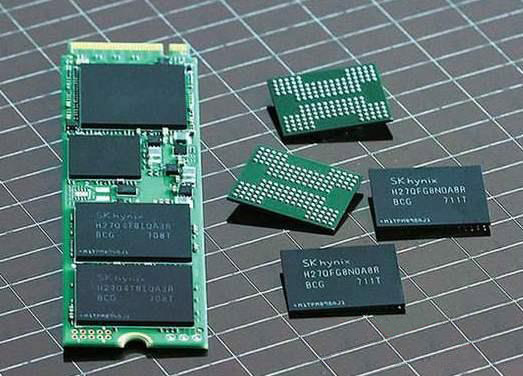
Yangtze Memory spans the 96-layer products and develops directly from 64-layer products to 128-layer products. It benefits from the assistance of Xtacking technology and is influenced by the boost of international competition. At present, leading international memory chip manufacturers including Samsung and SK Hynix have all launched 128-layer products.
For example, SK Hynix has delivered engineering samples based on 128-layer 1Tb 4D NAND to customers at the end of last year, and recently launched an enterprise level SSD based on the first 128-layer 1Tb TLC 4D NAND flash memory. Samsung had started mass production of 250GB SATA SSD, which use the 128-layer technology, in the middle of last year, and mass production of the 6th generation 128-layer 512Gb TLC 3D NAND was realized by the end of the year. For Kioxia and West Digital, the 512Gb BiCS5 TLC was successfully developed in the beginning of this year, and plans to launch 112-layer 1Tb TLC and 1.33Tb QLC.
As a rising star, Yangtze Memory has successfully mass-produced 64-layer 3D NAND since September last year, and became the first domestic storage manufacturer that successfully include a customer base in China. After 7 months, it has brought a new breakthrough. Yangtze Memory joined the competition of 3D NAND from the 32-layer technology. At that time, the technology gap with competitors was 4-5 years. After developing the 64-layer technology, the gap was shortened to 2 years.
However, the density of Yangtze Memory’s 64-layer product is actually equivalent to the density of competitor’s 96-layer products, so the real technology gap is actually smaller. And its announcement today that it has successfully developed 128-layer products marks that it has caught up with the industry mainstream, Yangtze Memory has developed its technology from 32-layer products to 128-layer products within 3 years.
Besides, since Micron and Intel have seperated, the two parties have also become independent in 96-layer 3D NAND technology and second-generation 3D XPoint technology. Recently, Micron said it will begin mass production of 128-layer 3D NAND based on a new architecture in the third quarter of this year and start commercial shipments in the fourth quarter, but did not disclose specific product details. According to foreign media reports, Intel plans to launch 144-layer 3D QLC NAND technology this year. Looking forward to hear more precise news from both sides.

In the shadow of the impact of the epidemic this year, Wuhan City, where the Yangtze Memory is located, was particularly nervous. The lock down of the city was eliminated on the 8th of this month, although the official announcement of full staff resumption and capacity utilization has reached 100%. However, because of the spread of the epidemic in the world over the past few months, market demand is still very low. Initially, the domestic consumer market was mainly affected by the epidemic, and now it is the overseas market that was affected by the epidemic.
For Yangtze Memory, the current 64-layer chip production capacity of the 12-inch fab is still in the growth period, and it is in the final research and development stage of 64-layer eMMC, UFS, SSD products. Mass production will start in the later half year when demand rise again, the product just happens to be scheduled on time.
The 128-layer products will bring greater value to its partners. Among them, the 128-layer QLC version will be the first to be applied to consumer SSDs, and gradually enter the fields of data centers and enterprise servers to meet the diversified data storage needs in future AI and 5G era. More importantly, QLC reduces the cost of NAND flash memory per byte and is more suitable to be large-capacity storage medium. With mainstream consumer SSD capacity reaching 512GB and above, QLC SSD has broad market application prospects in the future.

Leave a comment