The Rise of Yangtze Memory: Lurking, Accumulating, Breaking Through

Starting Point:

Survival in the Cracks – The Beginning of Domestic Storage

In the storage industry, high technical barriers, large capital investments, and long R&D cycles have always been the three core thresholds restricting new players.Since the 1980s, the memory chip market has gradually formed a “tripolar pattern”: Samsung, SK Hynix, and Micron have occupied the main share, firmly controlling the core technology and market pricing power of memory chip manufacturing. Samsung’s 3D NAND, SK Hynix’s LPDDR, and Micron’s enterprise-level SSD solutions have monopolized the upstream and downstream of the consumer and enterprise markets in China.Faced with the monopoly of international giants, the difficulties faced by domestic storage in the initial stage can be summarized as “lacking technology, lacking talent, lacking funds, and lacking trust”.

Lacking Technology: In the field of memory chip design and manufacturing, domestic enterprises started late, and in the early stage, they were mostly concentrated in the low-end market, lacking advanced process and product design capabilities. The lack of technological accumulation made domestic manufacturers unable to compete with international giants like Samsung in the mainstream market.

Lacking Talent: The core technology R&D of the memory chip industry requires a large number of high-end talents, and at that time, China’s technical reserves and educational resources in the semiconductor field were still unable to meet the demand.

Lacking Funds: The R&D and mass production of memory chips require huge capital support, and the R&D investment of international giants is often dozens or even hundreds of times that of domestic enterprises. Samsung’s R&D investment in the storage field exceeds 10 billion US dollars every year, while the R&D budget of domestic manufacturers is only a fraction of it. At the same time, the memory chip industry has a significant economies of scale effect, and domestic enterprises with insufficient production capacity face great challenges in cost control and market competitiveness.

Lacking Trust: In the early market promotion, domestic storage brands were often regarded as low-end substitutes by consumers. Due to limited technical capabilities, the performance, stability, and durability of early products were significantly different from international brands. This brand trust crisis further restricted the breakthrough of domestic manufacturers in the high-end market.

Most early domestic SSDs relied on imported chips for packaging and production, with representative manufacturers such as Galaxy, Team, and Maxsun. Their products were often labeled as “low-end substitutes”. In early user feedback, domestic SSDs were “full of problems”.

Short Life: The early versions of flash memory particles had unstable life, often damaged after two or three years of use.

Poor Performance: Limited by the optimization capabilities of controllers and firmware, the continuous writing speed and random read-write performance of early SSDs were far inferior to international giants.

Uneven Quality: Some products even had large-scale repairs due to non-uniform production standards.

In 2015, a domestic storage company tried to launch its own branded SSD, but due to the use of outdated process technology, the product speed could not even catch up with Samsung’s mid-range model three years ago.

An engineer recalled: “Before the release, we were full of hope, but after the release, the reputation was negative, and even the advertising slogan became a joke in the industry.” Such failure cases were not uncommon at the time.However, domestic brands did not give up because of this. They gradually accumulated experience in the early trials and errors, laying the foundation for subsequent development.

Lurking: Policy Promotion and Technological Accumulation

At the same time, the “invisible hand” began to layout.

In 2014, the State Council issued the “National Integrated Circuit Industry Development Promotion Outline”, proposing to achieve autonomous and controllable goals in key areas of integrated circuits by 2030, with memory chips listed as one of the priority support directions. Under this policy background, the domestic storage industry ushered in unprecedented development opportunities.

Establishment of National Fund

To promote the development of the semiconductor industry, the National Integrated Circuit Industry Investment Fund (referred to as the “Big Fund”) was established in 2014, with a total fundraising of 130 billion yuan. The Big Fund provided key capital support for domestic storage manufacturers, especially the continuous investment in Yangtze Memory, which laid the foundation for its technology research and development and capacity expansion.

Local Government Support

In addition to national policies, local governments also support the development of local storage industries by setting up special funds, providing tax incentives, and talent introduction plans. For example, Yangtze Memory’s headquarters is located in Wuhan, and the Hubei provincial government has provided a number of policy supports for its project construction, helping it to start quickly in terms of funds and resources.

Technical Blockade Stimulates Innovation

The intensification of technology competition across the ocean has made Chinese enterprises face stricter technical blockades. This external pressure has instead stimulated the independent innovation motivation of domestic manufacturers, making them have to take a different technical path from international giants.

Establishment and Technical Path Selection of Yangtze Memory

As the leading enterprise in the domestic storage industry, Yangtze Memory has established a strategic direction of “starting from basic technology research” since its establishment in 2016.

The early goal of Yangtze Memory was not high, but focused on the technical verification of a 32-layer 3D NAND chip.Although this product’s performance is hard to compare with Samsung’s 64-layer chip at the same period, its significance lies in that it is the first time for Chinese storage enterprises to achieve autonomous control from design to manufacturing.

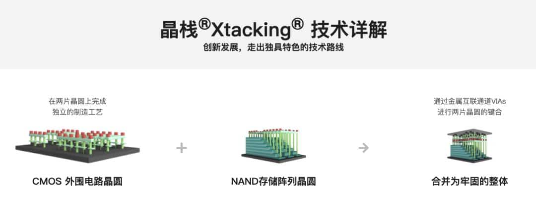
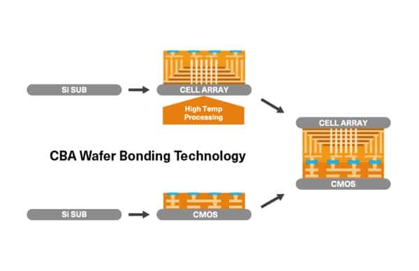
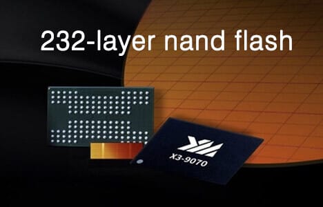
In 2018, Yangtze Memory released the world’s first Xtacking architecture technology. This technology not only improves the performance of memory chips but also significantly reduces manufacturing complexity and cost by separating the storage units and peripheral circuits and integrating them with vertical interconnection technology. This technological breakthrough has made Yangtze Memory shine in the global storage market.However, at the beginning of technology research and development, the challenges were huge.

In 2017, when the first generation of Xtacking chips was trial-produced, the yield was very low, and the product was almost difficult to mass-produce.

An engineer mentioned: “At that time, the lights of the whole building were often on until two or three o’clock in the morning, and many people even worried whether this technical direction was feasible.”However, after three years of continuous optimization and attempts, Yangtze Memory launched its first self-developed 64-layer 3D NAND flash memory chip in 2019 and quickly applied it to the consumer SSD market.

Although there is still a gap in performance and reliability compared with international brands such as Samsung, its cost performance advantage and local supply chain strategy have won a certain market share for it, and also made domestic storage have the foundation to compete with international giants for the first time.

Breaking Through: Technological Breakthroughs and Market Expansion

In the development process of Yangtze Memory, the Xtacking architecture is the most important technological milestone. The introduction of this technology not only marks Yangtze Memory’s transition from technological catch-up to independent innovation but also changes the global NAND flash memory industry’s technological competition landscape.

Lorem ipsum dolor sit amet, consectetur adipiscing elit. Ut elit tellus, luctus nec ullamcorper mattis, pulvinar dapibus leo.

The Xtacking architecture adopts a separate design for storage cells and peripheral circuits, efficiently integrating the two parts through vertical interconnection. This technological path brings many advantages.

Performance Improvement: Xtacking optimizes signal transmission speed, achieving higher random read-write speeds and lower latency. Compared with traditional designs, its performance improvement can reach more than 20%.

Manufacturing Efficiency: This architecture simplifies the production process, allowing wafer manufacturing and packaging testing to be carried out simultaneously, significantly shortening the production cycle.

Design Flexibility: Storage cells and peripheral circuits can be optimized separately, supporting higher-density storage cell stacking and increasing chip storage capacity.
With the support of Xtacking technology, Yangtze Memory quickly launched multiple generations of products.

In 2019, the first 64-layer 3D NAND chip was released, laying the foundation for the mass application of domestic NAND products.In 2020, the 128-layer 3D NAND was launched, reaching a global advanced level.

In 2022, the 176-layer 3D NAND was successfully developed, beginning to enter the high-end storage market and directly competing with Samsung and other international giants.These technological breakthroughs have enabled Yangtze Memory to have real competitiveness in the global market for the first time and have created favorable conditions for the rise of its retail brand, Zhitai.

Unlike early domestic SSDs, Zhitai has achieved a qualitative leap in quality, performance, and after-sales service.When the Zhitai SSD product TiPlus5000 was released, the market response was positive. Although it is still not as fast and performant as Samsung, its price is more attractive, and the cost-performance advantage is obvious.

In 2023, Zhitai released the TiPlus7100 series. This product is equipped with Yangtze Memory’s 128-layer 3D NAND chip, with continuous read-write speeds reaching 7100MB/s and 6500MB/s, not only catching up with Samsung’s flagship products but also performing excellently in terms of life and stability.

Once released, this product caused a warm response in the domestic market and became a star product on the JD platform.

In 2024, the performance of Zhitai during Double 11 became an important symbolic event in the development of the domestic storage industry:online SSD category Double 11 promotion total transaction amount (GMV) and sales double champion!

Zhitai’s JD transaction amount increased by 40% year-on-year, and total sales increased by 15% year-on-year. Among them, Zhitai TiPlus 7100 became one of the most popular explosive SSD products on the JD platform.

Specifically, the main reasons for Zhitai to surpass Samsung during Double 11 slaes promotion can be

Attributed to the following key factors:

Significant Price Advantage: During the 2024 Double 11 period, Zhitai attracted a large number of consumers through direct discounts and full reduction activities. During Double 11, many international first-line brands did not have price reduction measures, and even a certain brand had the operation of raising prices first and then returning to the original price.

Technology Empowers Promotion: Through social media, live streaming, and other forms, the advantages of Xtacking technology are transformed into selling points that consumers can perceive (such as faster transmission speeds, longer service life).

Service and Channels: Through JD’s self-operated and official after-sales support, the problem of low consumer trust in early domestic brands was solved.

Behind these data is a comprehensive breakthrough of Yangtze Memory and Zhitai in technology, brand, and market.

Rise: The Logic Behind and Industry Significance

The fundamental reason for Yangtze Memory’s rapid rise is its persistence and breakthrough in technological innovation.

The release of the Xtacking architecture has broken the traditional design thinking of the storage industry, raising the performance and manufacturing process of NAND flash memory to a new level. In the global storage industry, the core of NAND flash memory technology is dominated by companies such as Samsung, Micron, and Intel, and domestic storage has always been in a technological catch-up situation.

However, Yangtze Memory has successfully filled the technological gap through independent research and development and technological breakthroughs, achieving the goal of “autonomous control.” From the successful development of 64-layer, 128-layer, to 176-layer 3D NAND flash memory, Yangtze Memory has not only solved the technical shortcomings of domestic storage but also broken the technological blockade of international giants, proving that China has the ability to compete with the world’s top enterprises in the field of semiconductor storage.In addition, its technology accumulation and rapid iteration strategy are also crucial.

In just a few years, Yangtze Memory has continuously optimized the Xtacking architecture, introduced new products, and launched multiple generations of products. This ability to rapidly iterate technology allows it to quickly adapt to market demand changes, ensuring product competitiveness. At the same time, Yangtze Memory’s large-scale production has also helped it maintain a technological lead, ensuring domestic market supply and competitiveness.

Policy Support and Industry Environment

The “invisible hand” has been paying increasing attention to the semiconductor industry. From the establishment of the “Big Fund” to the local government’s support for the storage industry, national policies have provided great financial and policy support for domestic storage manufacturers. These supports not only help enterprises with technology research and development but also provide a more relaxed market environment for them.In addition to national policy support, local governments have also played an active role in promoting the development of the semiconductor industry.

As a key project supported by Hubei Province and Wuhan City, Yangtze Memory has received full support from local governments in terms of funds and talent introduction. This close cooperation between government and enterprises has prompted the domestic storage industry to complete the leap from technological catch-up to leadership in a short period.Moreover, the collaboration of the upstream and downstream of the industry chain has also provided a solid foundation for the development of domestic storage. The continuous improvement of materials, equipment, and packaging testing links has greatly enhanced the competitiveness of the domestic storage industry.

From the initial technological lag and market downturn to breaking through the encirclement through policy support, technological innovation, and brand promotion, domestic storage enterprises have gradually become an important force in the global storage industry. The success of Yangtze Memory and Zhitai marks the technological breakthrough of the domestic storage industry, but future competition is still full of unknowns.

Major personnel changes at Samsung Electronics

On November 27th, Samsung Electronics announced routine personnel changes for the 2025 class of presidents, totaling 9 individuals, with 2 being promoted to president and 7 experiencing role changes.

Samsung, in crisis, has implemented a reorganization of its presidency, focusing on the memory semiconductor business.

Moving forward, the memory business will be directly managed by the CEO and vice chairman, without a separate president position.

In the regular 2025 president reshuffle, Samsung Electronics appointed Vice Chairman and head of the Device Solutions (DS) division, Jeon Young-hyun, as CEO, aiming to revive the semiconductor business.


The Device Experiences (DX) division remains under the leadership of CEO and Vice Chairman Jong-hee Han, with Vice Chairman and head of the Business Support Task Force (TF) Hyun-ho Jeong retaining his position, solidifying the vice chairman system.

The personnel changes include: transforming the memory division into a system directly under the CEO’s jurisdiction, replacing the foundry (contract manufacturing) business leader, and appointing an experienced and mature CEO to manage new businesses. To overcome uncertain internal and external business environments and achieve new leaps, a personnel reform has been announced, including the allocation and mining of tasks.

Additionally, to strengthen semiconductor technology competitiveness and renew the organizational atmosphere, we have established a president-level CTO position in the foundry division and a president-level management strategy position directly under the DS division, empowering senior presidents with authority. Challenges such as brand and consumer experience innovation have been introduced to improve the company. The company announced a focus on enhancing its medium and long-term value.


Among them, Jinman Han, Vice President of the DS Americas (DSA) division responsible for the semiconductor business, has been appointed as the president of the foundry business division. Jinman Han has served as the head of DRAM and flash memory design teams, SSD development teams, and the Strategic Marketing Office, and was appointed as the head of the Americas region at the end of 2022, leading the semiconductor business at the forefront. With his combination of technical expertise and business acumen, along with extensive experience dealing with global customers, it is expected that he will enhance the competitiveness of the foundry business through process technology innovation and strengthening networks with key customers.

Kim Yong-gwan, a member of the Business Support Special Task Force (TF) and vice president, has been promoted to the position of President of Management Strategy for the DS division. Kim Yong-gwan, after working in semiconductor planning and finance, and in the Strategy Group and Management Diagnostics Group of the Future Strategy Office, moved to the Business Support TF in May, responsible for semiconductor support, and is expected to play a leading role in the early recovery. It is reported that Samsung has indicated an intention to enhance semiconductor competitiveness through this forward deployment.

Vice Chairman Jeon Young-hyun, who is also the head of the DS division, serves as Samsung Electronics’ CEO and head of the DS division, memory business division, and SAIT President.

The CEO of Samsung Electronics has traditionally been a vice chairman. In particular, the DS division is generally led by executives such as Chang Kyu Lee and Ki Nam Kim.

Under the leadership of former DS division head Chang Kyu Lee, he unusually held a president-level position, but in May of this year, Vice Chairman Jeon Young-hyun took over the organization again and elevated the status of the president.

Samsung Electronics is expected to shift from a single CEO system led by the DX division head (Vice Chairman) Han Jong-hee to a dual CEO system, including the former vice chairman, thereby enhancing the competitiveness of the semiconductor business. Samsung Electronics explained that the reason for restoring the two-person system of CEO and vice chairman is “to establish a business responsibility system for each division.”

Nam Seok-woo, CEO of the Global Manufacturing and Infrastructure Headquarters of the DS division, has been transferred to the position of Chief Technology Officer (CTO) of the foundry division.

It is noteworthy that a direct system with the CEO also serving as the head of the business division has been established.

Most importantly, as Samsung Electronics’ memory division has ceded leadership in the high-bandwidth memory (HBM) and other artificial intelligence (AI) memory markets to competitors, a seasoned senior leader seems to have issued a special command to directly lead the division.

Jong-hee Han, Vice Chairman and head of the DX division and Home Appliances (HA) division, will also serve as the chair of the newly established Quality Innovation Committee.

This is seen as a determination to fundamentally prevent quality disputes over Samsung Electronics’ products, in light of recent quality controversies surrounding the Galaxy Buds.

Lee Young-hee, head of the Global Marketing Office and Global Brand Center of the DX division, has been appointed as the chair of the Brand Strategy Committee.

Wonjin Lee has been appointed as the head of the Global Marketing Office of the DX division. Wonjin Lee, a Google advertising and services business expert consultant, resigned from his position as the head of the service business team in the Mobile Experience (MX) division at the end of last year and will return to the management frontline after a year, serving as the head of the global marketing department, overseeing marketing, branding, and online business.

Koh Han-seung, CEO of Samsung Bioepis, has been transferred to the position of head of Samsung Electronics’ Future Business Planning division.

Park Hak-gyu, head of the Management Support Office of the DX division, has been transferred to the position of president, responsible for Samsung Electronics’ business support TF.

Samsung Electronics usually appoints presidents in early December, but this year, like last year, it was advanced by about a week.Previously, Samsung Electronics Chairman Lee Jae-yong stated in his final remarks at the second trial on November 25th, “I am well aware that there has been a lot of concern about the future of Samsung recently, and the reality we are facing now is more difficult than ever, but this is a difficult situation.

I will definitely overcome this and take a step forward.” He continued, “Please give us the opportunity to overcome this difficult situation and become a Samsung loved by the people.”

Therefore, following the personnel changes of the chairman, there is a high possibility of executive personnel and organizational restructuring in the near future.

Due to unfavorable internal and external situations, the scale of executive promotions is expected to be reduced compared to previous years.Samsung Electronics plans to complete personnel and organizational restructuring and hold a global strategy meeting in mid-December to discuss next year’s business plans.

SK Hynix Q3 FY24

Hynix’s Q3 Quarterly Financial Report and Procurement of HBM Equipment

Hynix Q3 Financial Report: Revenue in the United States Reaches 64%, China Decreases to 24%.

Unlike semiconductor equipment manufacturers such as ASML, which are significantly affected by fluctuations in China, SK Hynix’s prospects appear optimistic, thanks to strong HBM demand in the United States.
According to South Korean media outlet newdaily, citing its quarterly report published on November 15th, the company’s sales in the United States hit a historical high in the third quarter as HBM3e is fully supplied to NVIDIA, and it is expected to maintain strong momentum throughout next year.


The report shows that the United States accounted for 64% of SK Hynix’s third-quarter sales, increasing by 5 percentage points from the previous quarter and 17 percentage points year-on-year, setting a historical high.

In monetary terms, in the third quarter alone, SK Hynix sold memory worth 11.327 trillion won (approximately $8.7 billion) to the United States, slightly less than the total sales in the United States in the first half of this year.

According to newsdaily, there is growing anticipation that SK Hynix’s sales in the United States will be even higher in the fourth quarter and next year, as NVIDIA’s upcoming Blackwell is expected to drive a surge in HBM supply starting from this quarter.As previously reported by Reuters and South Korean media ZDNet, NVIDIA CEO Jensen Huang requested SK Hynix to advance the supply of HBM4 by six months.

The company stated in October that it plans to deliver chips to customers in the second half of 2025.According to ZDNet, to further capitalize on opportunities in the U.S. market, the memory giant established a new subsidiary in Indiana in the third quarter after securing funding under the CHIPS Act to build an AI memory advanced packaging production facility in the United States.

According to SK Hynix’s press release, the Indiana factory is expected to begin mass production of next-generation HBM and other AI memory products in the second half of 2028.On the other hand, China once accounted for about 30% of SK Hynix’s regional revenue, but its share dropped to only 24% in the third quarter.

According to the report, this situation can be attributed to two reasons. First, as SK Hynix’s Chinese customers focus on personal computers, smartphones, and IT devices that use general-purpose memory, the demand for traditional memory products has decreased, and China’s contribution to SK Hynix’s total revenue seems to be weakening.

Furthermore, it is reported that ongoing regulatory pressure from the United States on China has also led to changes in SK Hynix’s revenue structure.

SK Hynix Procures Nearly 58 Million in HBM Equipment!

Semiconductor equipment company Yest demonstrates its strength with news of supplying to SK Hynix.

According to the South Korean stock exchange on November 20th, as of 11:16 AM, Yest’s trading price was 9,160 won, up 7.76% from the previous trading day.

After continuing a sluggish performance due to concerns about a slowdown in the semiconductor industry and the “Trump shock,” Yest seems to have successfully rebounded and returned to the 10,000 won mark.

Yest announced earlier in the day that it had signed a contract to supply high-bandwidth memory (HBM) semiconductor manufacturing equipment to SK Hynix, and its stock price soared to 9,490 won.

Yest will supply electric furnaces worth 11.16 billion won (57.59 million yuan) to SK Hynix, which are key equipment in the HBM production process.

Yest’s semiconductor furnaces are equipment that use the radiated heat from heaters to remove impurities or stabilize the structure of wafers during the semiconductor manufacturing process.

Securities firms are concerned that the South Korean semiconductor industry may lose its leading position in the future.

Daol Investment & Securities researcher Ko Young-min stated, “South Korea’s leadership in the semiconductor field will be solid until 2026, when the semiconductor cycle will continue because significant technological inflection points will arrive within three years, and we must be vigilant about latecomers developing innovative technologies.”

STM32 Demo Board: Getting Started and Advanced Preparation

Essentials for Beginners

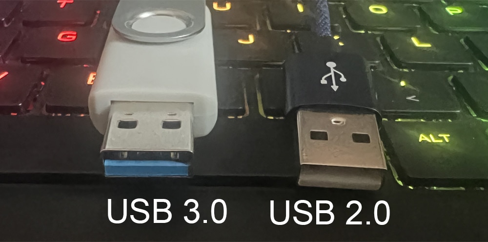
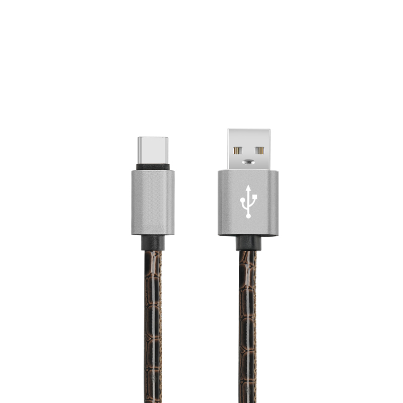
The development board may look simple, but many people are discouraged at the step of how to use it. Today, I’m here to teach you how to solve the problems of getting started with single-board computers (SBCs), taking the Orange Pi Zero 3 as an example. How many steps are generally needed to use an Orange Pi? First, prepare a USB Type-C power cable, a charger with at least 5V 2A , a memory card with a capacity of at least 8GB, and a Micro HDMI cable to connect to a monitor or TV to display information from the development board. Some Demo Boards may have DP or mini HDMI interfaces, or standard HDMI interfaces, and you will need to purchase the corresponding cables to match your development board.

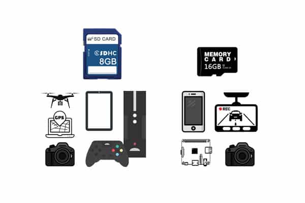
custom Micro SDHC card 16GB
If your monitor doesn’t have a DP interface, you can opt for a DP-to-HDMI cable. However, as of now, there are still few Demo Boards without an HDMI interface. We also need to prepare a keyboard, and if you’re using a desktop like Windows, you’ll also need a mouse. If your Demo Board doesn’t have WiFi or Bluetooth, you’ll need to provide an Ethernet cable and access to the internet. Finally, you’ll need a working computer with a USB port. If your Demo Board has onboard eMMC, you won’t need to prepare a TF card. If your development board also has an M.2 SSD interface and you happen to want to use an SSD, you’ll also need to prepare an SSD.

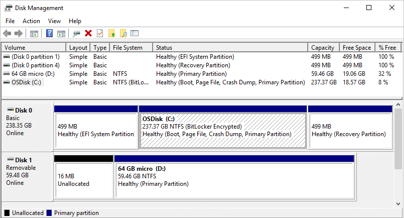
After preparing all this hardware, the next step is to install the system. Installing a system on a development board is simpler than on a computer. First, find the official website of the development board and download the system you want to use onto your computer. Then you can proceed to install the system. There are several installation methods, which differ depending on which storage medium you want to install the system on, such as a memory card, eMMC, or SSD. Installing on a memory card is the simplest.

Here, pay attention to the protocols and sizes of the SSDs supported by the development board. There are two protocols: M.2 SATA SSD interfaces and NVMe SSD interfaces. In terms of size, they vary based on length with M.2 2230, 2242, and 2280 being the main sizes. You need to choose the SSD based on the protocols and slots provided by the development board.

Pay attention to the protocols and sizes of the SSDs supported by the development board. There are two protocols: M.2 SATA SSD interfaces and NVMe SSD interfaces. In terms of size, they vary based on length with M.2 2230, 2242, and 2280 being the main sizes. You need to choose the SSD based on the protocols and slots provided by the development board.

Flashing the system to the SSD is also done using the Ralink development tools, with the difference being the configuration file; just select PCI and the system installation is complete.

Once the hardware and software are ready, plug in the HDMI and power cables and wait for the system to boot. Note that some Demo Boards have a switch, which could be a selection switch or a push-button switch, so you should refer to the documentation for operation. Generally, the system will start automatically when powered, and if it doesn’t start automatically, check if the switch hasn’t been pressed.

Professional Player Essentials

Some commonly used tools in electronic design, which can also be considered essential, start with soldering. First is the soldering iron, which comes in temperature-controlled and adjustable temperature models. A temperature-controlled soldering iron is similar to this type where you plug it in and it directly reaches a fixed temperature.

The higher the wattage, the faster it heats up. An adjustable temperature soldering iron is similar to this type, generally adjustable between 200 to 500 degrees, because some chips have requirements for soldering temperature and cannot withstand high temperatures, so this adjustable temperature soldering iron has a broader range of applications. When using a soldering iron, you need a soldering iron stand, which comes in various types and can be chosen based on personal preference.

Soldering Iron

When using a soldering iron, you need to frequently clean the tip, which is where the soldering sponge comes in, similar to the one in the picture. Then there’s solder, which comes in leaded and lead-free varieties, with different tin content and wire gauges. I personally often use 63/37 tin with a 0.6mm diameter.

There’s also flux in the form of solder paste or rosin, solder paste is similar to the one in the picture. Rosin is similar to this type of desoldering pump. When soldering and needing to remove some solder, a desoldering pump is needed, which looks like the one in the picture. Then there’s the solder wick, which is this type of perforated board, but it’s basically disposable, and after soldering, it’s hard to clean and reuse.

Breadboard

A breadboard is a type of board where you can insert components and perform some debugging and testing.

Dupont Wire

Dupont wires are used to connect two endpoints of a test circuit, generally divided into male and female ends, with the female end being this type with holes and pins. Choose according to your needs, and the male end looks like this, which is also a commonly used small tool in testing circuits. You can insert Dupont wires or their corresponding sockets, and this is the socket corresponding to the pins.

Tinned Wire

Then there’s tinned wire, also known as enameled wire, which comes in different thicknesses and lengths, and is also commonly used in testing to connect two solder points.

Others

Tweezers are used as conductors for adding small precision components, and small surface-mount resistors and capacitors are commonly used. Flush cutters are used for trimming, similar to this type, generally for cutting the leads of some soft components. To strip the outer skin of wires, you need wire strippers, which are also commonly used.

A multimeter is also the most commonly used tool for measuring current, voltage, resistance, capacitance, and continuity, which can be said to be the most commonly used tool in electronic design.

Conclusion

Then there are some tools that are not commonly used at the beginning of electronic design, but can be added later when needed, such as hot air guns, needle-nose pliers, screwdrivers, some fixtures, heat shrink tubes, regulated power supplies, oscilloscopes, and logic analyzers. Basic electronic design may not need these for the time being.

This article introduces how to choose and use STM32. It is hoped that through the introduction in this article, beginners can understand the basic concepts and entry guide of STM32 for subsequent learning and application. If you don’t understand embedded systems, come to me. Thank you, everyone.

SK Hynix’s NAND FLASH

SK Hynix’s NAND FLASH Market Share to Exceed 20% for the First Time

SK Hynix’s global NAND flash memory market share is expected to surpass 20% for the first time this year. SK Group Chairman Chey Tae-won has decided to take personal charge of the NAND business, which is expected to accelerate the process of narrowing the gap with market leader Samsung Electronics.Industry insiders stated on November 18th that SK Hynix’s global NAND market share, calculated by sales (according to IDC statistics), has increased by more than 10 percentage points over the past four years, growing from 11.7% in 2020 to 22.5% in the second quarter of this year. Although SK Hynix acquired Intel’s NAND division and launched Solidigm in 2021, the expansion of its market share was not as rapid as anticipated, rising from 13.7% in 2021 to 19% in 2022, but almost stagnating at 19.2% last year. The semiconductor economic downturn had a significant impact on Solidigm’s ongoing deficits.
SK Hynix’s NAND FLASH
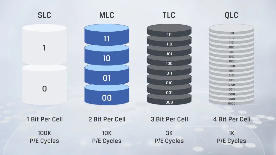
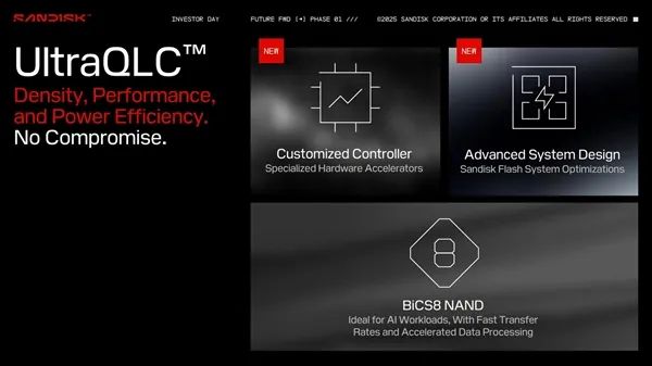
Solidigm has steadily reduced its deficits and successfully turned a profit in the second quarter of this year (net profit of 7.86 billion won). Due to increased investment in AI data centers, the demand for high-capacity enterprise SSDs (eSSDs) has surged, and Solidigm’s competitiveness in this market has been rewarded. Only Samsung Electronics and Solidigm possess quad-level cell (QLC) NAND technology. NAND is categorized into SLC, MLC, TLC, and QLC based on data storage methods. Compared to SLC with the same cell, QLC can store four times more data, easily achieving high capacity and improving production cost efficiency.Due to sluggish demand in PCs and mobile devices, SK Hynix’s NAND shipments in the third quarter decreased compared to the previous quarter. However, profitability was maintained at a level similar to the second quarter because the average selling price (ASP) of high-value eSSDs increased by about 10% from the previous quarter. eSSDs accounted for more than 60% of SK Hynix’s NAND sales in the third quarter.Thanks to the continued strong demand for eSSDs, SK Hynix’s annual NAND market share this year is expected to exceed 20% for the first time. During a conference call to announce the third-quarter results, SK Hynix stated, “Although the NAND market share calculated by volume may decrease this year, we anticipate an increase in the market share calculated by sales compared to last year.”SK Hynix is poised to accelerate the reduction of the market share gap with Samsung Electronics, whose NAND market share is in the mid-30% range. SK Hynix aims to increase its market share with a focus on high-value products such as high-capacity eSSDs. The company recently launched a new eSSD product capable of achieving 122TB, the largest capacity for NAND solutions. There are also predictions that with Chairman Chey Tae-won recently taking over as the chairman of the Solidigm board, the NAND business will be further strengthened.

HUAWEI eKitStor Xtreme 200E SSD Prospective Evaluation and testing

Xtreme 200E SSD,Today’s topic is about Huawei’s new solid-state drive (SSD). We have obtained a prototype of Huawei’s SSD that has not yet been released (it will be officially launched at the end of November). However, there is essentially no difference between this engineering sample and the final version, except for the serial number. It’s a 1TB single-sided chip SSD. Let me tell you, getting this SSD was quite an effort. Let’s see what secrets are hidden under this label. It’s just a regular sticker and does not serve any cooling function.


For the 1TB capacity, there are two chips and one controller, which is a standard DRAM-less solution. It’s not easy to distinguish the manufacturer of the chips from the numbering. Without further ado, let’s compare it with the Zhitai Ti600, which is also a popular SSD sold online. Through comparison, we can confirm that Huawei’s new SSD definitely does not use the Lian Yun controller, and it is even less likely to use controllers from Samsung, Phison, or Silicon Motion. So, there should be only one answer in our minds.

Warranty

Nice, in terms of warranty, Huawei offers a 400TBW warranty for the new SSD, coincidentally, the Zhitai Ti600 also offers a 400TBW warranty. It is also unlikely that Huawei would use storage chips from Micron, Samsung, or Kioxia. So, the answer in front of us might be the one we all have in mind. In terms of price, I estimate that it should not be too expensive.

Testing

The SSDs tested together are: Kioxia RC20 1TB and Western Digital SN850 1TB. First, we clarify that this test will not do Huawei’s SSD any injustice. Both SSDs tested alongside are flagship SSDs with cache. Looking at the basic parameters, the PCIe-4.0 x 4 full-speed is flawless, with sequential read speeds of 7100 and sequential write speeds of 6300, which is a pretty good performance. Digital novices like to focus on this parameter, and the commonly used 4k91mb and 286mb performance is basically enough for daily use. This data is also basically consistent with Zhitai’s Ti 600, and we need to look at the 200GB+ mixed data write test.

SSD Cache

Why test 280GB? Because I initially thought it would have a 200GB cache, like the Zhitai Ti600. But after testing, the speed did not drop, and the cache was quite large. We directly increased it to 280GB to test the cache. Huawei’s SSD has a full-disk simulated cache of 250GB, and data exceeding 250GB will experience a decrease in transfer speed, and it will experience a speed drop. A 250GB simulated cache in an empty state is indeed very large, and it is completely sufficient for our daily home use. However, it is still a QLC chip after all.

After the Huawei SSD is half full, the mixed test shows that the 200E SSD only lasted 20GB before the cache was released, which is a common issue with QLC DRAM-less SSDs. That’s just how it is. Don’t understand? Let’s look at the actual performance. When we control the disk and copy 200GB of data, the read speed is relatively stable, basically around 3.6GB, and the entire copy time is around 55 seconds. The 200GB is copied, very fast, no problem at all.

Application Scenarios

If your SSD is already half full, and you copy files again, you will find that it is very easy to release the cache at this time, and the speed will be similar to your home mechanical hard drive when the cache is released. Therefore, the Huawei 200E SSD, because it is equipped with QLC chips, although its controller is strong, the storage chips are too ordinary. The most suitable group of people is ordinary home users who do not store too many things, and the 1TB capacity can be used for several years. So, this SSD is no problem at all, so it feels like the storage chips are holding back the controller.

Self-developed Chips

However, considering the current market environment and what tricks Trump might pull after he comes to power across the sea, no one knows what kind of environment it will be after Trump comes to power. We should encourage any brand or group in China that wants to do something from 0 to 1. Products need to be developed one by one, and the market needs to be developed bit by bit. We also hope that Huawei will release some PLC or higher-performance SSDs in the future, after all, the step from 0 to 1 is the most critical. This is what I mentioned at the beginning of the article, that the price of this SSD should not be too expensive. So, above is the prospective review of Huawei’s new 200E SSD. If you have any opinions on Huawei’s new SSD, you can also leave a comment. I am Teacher Alex, see you next time.

chip sales by area

The changes in the semiconductor industry in 2024 are greater than the sum of the changes over the previous five years combined.

In 1995, Nvidia’s first chip, the NV1, faced numerous setbacks, leaving the company with only 30 days of working capital. By 2024, Nvidia’s Blackwell GPU was in such high demand that the company’s market value had surpassed $3.6 trillion. Also in 1995, Intel held over 75% of the global PC processor market, establishing its leadership in the personal computer market. Fast forward to 2024, Intel’s stock price has plummeted nearly 60% since the beginning of the year, with its market value dropping to over $80 billion, marking the first time in three decades that it has fallen below the $100 billion threshold. The changes in the market values of these two semiconductor giants are a microcosm of the current semiconductor landscape.There is a saying that goes, “People tend to overestimate the changes that happen in a year, but underestimate the changes that happen in five years.” Looking back, the changes in the semiconductor industry in 2024 have been greater than the sum of the changes over the previous five years. 2024 will be a turning point for the semiconductor industry. Why do we say that? Because, as an industry, the semiconductor sector is inseparable from the basic characteristics that define it: division of labor, products, and services. And products like computers and chips cannot be separated from the science behind them. The industry and science are interdependent, and even before the 1970s, the industry was clearly dependent on science. (The controversy over the Silliman affair was a watershed in the relationship between science and industry.) The significant changes in the semiconductor industry this year are the result of a three-way tug-of-war between technology (science), policy, and the market.

01 The Transformation of Semiconductor Companies

In 2024, there have been many news items that have stimulated the nerves of industry insiders. The most prominent is still the surging market value of Nvidia. Microsoft and Apple have been the two companies with the highest market value in the world since 2010. Although the two have been “entangled” in the ranking of “U.S. stock market leader” for more than 10 years, no one else has replaced them. On June 18, 2024, local time, Nvidia’s stock price rose by 3.51%, closing at $135.58, with a total market value of $3.335 trillion, surpassing both Microsoft and Apple to become the company with the highest market value in the world. This is a change that affects the whole world, such as in August 2011 when Apple first defeated ExxonMobil to win the title of the world’s most valuable company, which was also a symbolic moment for technology companies to defeat traditional oil companies. And Nvidia becoming the world’s most valuable company represents a shift in the focus of technology industry development. Traditional fields represented by Apple, such as consumer electronics and software, have led an era in the past, while Nvidia’s first place means that the focus of technology industry development is accelerating towards the AI field. In addition, on November 8th of this year, Nvidia replaced Intel as a component of the Dow Jones Industrial Average. S&P Global stated that the adjustment of components is to ensure that the index has a more representative semiconductor exposure. In fact, this is also proof: AI has truly entered the commercial track, and the impact of AI on the semiconductor industry is growing. In the semiconductor industry in 2024, in addition to the continuously increasing upper limits, there are also constantly refreshed lower limits. There are two giants in the semiconductor industry, which are well-known to everyone: Intel and Samsung. Since 1992, Intel has been the world’s largest semiconductor manufacturer and has been leading for 25 years. Although Samsung’s chip business surpassed Intel for the first time in 2017, it is still a constant struggle for the leading position. This year’s two chip giants seem to be stuck in a “swamp,” constantly struggling. As mentioned earlier, Intel’s market value has fallen due to its continuously losing performance. In the second quarter of this year, Intel’s loss reached $1.6 billion, far higher than the loss of $437 million in the previous quarter. And the latest third-quarter financial report announced its largest quarterly loss in its 56-year history – $16.6 billion (about 118.2 billion yuan). Samsung is also in a difficult situation in 2024. In October, Samsung announced that its third-quarter operating profit was about 91 trillion won, lower than the market expectation of 115 trillion won. Jeon Young-hyun, head of Samsung’s electronic device solutions department, also issued an apology, stating that the company’s performance did not meet market expectations, causing people’s worries about the company’s basic technical competitiveness and the future. As the senior management leading the company’s operations, they will take responsibility. (It seems that South Korea has also learned the apology system from Japan.) Similarly, the stock market reflects the company’s situation. Samsung’s stock price fell to 51,700 won on November 14th, local time, a record low since June 24, 2020. If this trend continues, Samsung’s stock price for the whole year will be the worst performance in over 20 years.

02 Europe’s “Decadence”

The changes in 2024 are not only the obvious corporate rankings but also regional changes. Amid global government attention to the semiconductor industry, there is a region where semiconductors have been declining throughout the year – Europe. Many people may not have noticed, but the data from WSTS cannot be deceived.
chip sales by area
We have calculated the chip sales announced by WSTS since January of this year, and so far, the chip sales in Europe for the whole year have been negative year-on-year. Of course, there is also Japan, but Japan’s year-on-year growth has slightly turned positive in August and September. The European semiconductor industry fell into a weak state in 2024. The “three giants” of the European semiconductor industry: Infineon, STMicroelectronics, and NXP, all have poor revenue. Infineon’s revenue in the third quarter reached 3.702 billion euros, a year-on-year decrease of 9%. Currently, Infineon has lowered its performance outlook for 2024, adjusting this year’s revenue expectation to 15.5 billion to 16.5 billion euros, lower than the previous expectation of 16.5 billion to 17.5 billion euros. STMicroelectronics’ net revenue in the third quarter was 3.25 billion US dollars, a year-on-year decrease of 26.6%. NXP’s revenue decreased by 5.4% to 3.25 billion US dollars, slightly lower than the analysts’ expected 3.26 billion US dollars. Nowadays, Europe’s automotive and industrial markets have already shown negative growth.
From a more specific level of observation, the performance of optoelectronics and discrete devices is not satisfactory, the MCU market shows a shrinking trend and has shown negative growth, and the analog market has also experienced a long period of decline.

03 Tracing Back to the Source

The only constant in the world is change itself. This year, there have been so many changes in the semiconductor industry. Let’s trace back to the root causes and examine policies, markets, and technology.

Revenue of the 2024 top 10 global semiconductor companies
2023 ranking 2024Q3 ranking Company Q3 revenue in 2024 Year-on-year revenue
5 1↑ NVIDIA 300.4(Q2) 122.40%
6 2↑ SKHynix 116.75(Q2) 124.79%
9 3↑ APPLE 857.77 4.87%
2 4↓ Samsung 560 7.35%
1 5↓ Intel 132.84 -6.17%
4 6↓ Broadcom 130.72 47.27%
3 7↓ Qualcomm 93.9 8.77%
7 8↓ AMD 68.19 17.57%
10 9↑ Texas Instruments 41.51 -8.41%
8 10↓ STMicroelectronics 32.51 -26.63%
Source: Financial Report Semiconductor Industry Vertical and Horizontal Tabulation

The impact of policies on the industry is self-evident. At the policy level, the United States, Europe, Japan, South Korea, and Vietnam have all released semiconductor-related policies in the past two years. However, looking at the current situation, the implementation of the semiconductor policies in the United States and Europe has not been significant.

So far, more than half of the $52 billion subsidy in the U.S. Chip Act has been allocated, with over $35 billion granted to about 26 projects. Yet, the funds seem to be slow in coming, with Intel constantly complaining, “It’s been two years, and we haven’t seen a penny.”

Policy

The U.S. Chip Act is even more precarious after Trump’s potential return to office next year, as he is known to be opposed to the act. In interviews, Trump has bluntly stated, “It’s terrible.” The European Chip Act has not made any waves either. Proposed in 2022, there are not many factories being built in Europe, and Intel’s project has not even started. However, it is important to note that the Chip Act has played a role in attracting investment without actual capital. Companies like Intel, TSMC, Samsung, Micron, GlobalFoundries, and Amkor have already begun constructing factories in various regions of the United States due to the subsidies from the Chip Act. Even if the timeline for financial assistance is extended or the subsidies are canceled, it is unlikely that the partially constructed fabs will become abandoned projects. It can be said that for semiconductor companies, building factories in the United States is already an inevitable action. Although the Chip Act has not been fully implemented and Trump denies its effectiveness, there is no doubt that he supports the repatriation of advanced manufacturing to the United States. This is why, when looking at Intel, we also believe that Intel will not be as bad as it seems. Despite Intel being constantly criticized, we cannot ignore its significant role on the geopolitical stage and as one of the U.S. government’s chips in the semiconductor industry and foreign policy strategies. When considering Intel’s prospects, we must not overlook the elements of U.S. strategy and geopolitics. The semiconductor industry now occupies an important strategic position, which is common knowledge. Regardless of whether it can reach the extreme 3nm process, globally, there are only three companies capable of manufacturing advanced process chips: TSMC, Intel, and Samsung. A significant part of the U.S. Chip Act’s plan is directed towards Intel’s construction of two large factories in Arizona and the building of two more factories in Ohio. Therefore, Intel’s future is still full of Highlights. It is not appropriate to directly assume that it will “decline to the end.”

Market

Why has the term “involution” started to be used domestically in recent years? It is because the pace of technological innovation has slowed down, and with the impact of the three-year pandemic, China’s economic development speed has also slowed down under various pressures, leading to “involution.” The “second curve” theory believes that industrial development has a life cycle, and any growth curve is a parabola that rises and then falls. The secret to sustained growth is to start a new growth curve before the inflection point appears, thus forming a continuous improvement and development trend with the new and old momentum in sequence. We are now in the depression period of the last round of technological and industrial revolutions. To make the economy prosperous again, a new round of technological and industrial revolutions must be ignited.This is the inflection point brought by the cycle. The new round of explosion is undoubtedly in AI, which is also a consensus among many industry insiders.

Tech

AI brings new growth points to the market, with many technologies hidden under AI. Above AI, we need to see the development of technology. The outbreak of AI this time is undoubtedly driven by technology. The emergence of GenAI has been brewing for a long time. And this outbreak of AI has driven other technologies that were brewing. The first representative is: TSMC’s advanced packaging process, CoWoS. The two most concerned products in the semiconductor industry: GPU, HBM, both of these products rely on advanced processes to be produced. And TSMC’s CoWoS packaging plays a very key role, so that some people have begun to jokingly call “TSMC will be the world’s first packaging and testing factory.” Here, the packaging and testing, which originally belonged to the back-end process, has shown a clear trend of front-end. And in the process of HBM suppliers continuously improving the stacking density, the interconnection between the fifth-generation HBM (i.e., HBM4) and the logic layer in the future will be jointly completed by storage giants and foundries. According to SK Hynix, HBM4 will greatly change the industry’s perception of DRAM as a “universal chip,” turning it into a customized storage special process chip. In this process, the related technical know-how will be jointly undertaken by foundries and storage factories, which is also the meaning of TSMC’s “Foundry 2.0” plan this year. The second representative is: the architecture competition, that is, the market competition between x86 and Arm, RISC-V. This year, it is obvious that the market share of Arm architecture chips is increasing. The x86 alliance has made it very clear not long ago: face to face. Although it seems to be a change in the market among the three architectures at first glance, it is actually a thirty-year-long competition between CISC (Complex Instruction Set) and RISC (Reduced Instruction Set), these two chip design philosophies. This competition is essentially an extension of the development of computer architecture as a “science and technology” in the “industry” field. The emergence of AI has given these two design philosophies more application scenarios. From the current point of view, the architecture under the RISC architecture (Arm, RISC-V) indeed has an innate advantage because it has the low power consumption and high energy efficiency that AI naturally needs. This also means that Arm may one day achieve a higher market share, which is driven by both technology and the market.

MLC 10000 write cycles, TLC 3000 to 5000 write cycles.

MLC Vs TLC, Is MLC Better Than TLC for SD Card?

MLC Vs TLC NAND Flash Memory Card

MLC Vs TLC,An SD card’s cost and storage are only part of the story. For essential data, understanding the NAND flash type—MLC or TLC—matters. These types affect speed and durability. This article explores them, helping you make the best choice.

MLC Vs TLC, Overview of MLC and TLC

In SD storage, the choice between MLC Vs TLC NAND flash impacts your card’s performance, lifespan, and cost. These flash types represent different data storage approaches, offering options tailored to specific user needs.

MLC 10000 write cycles, TLC 3000 to 5000 write cycles.

What is a Multi-Level Cell?

MLC, storing two bits per cell, offers a balance of speed and durability. This type works well for users needing moderate performance without a premium price.

Why MLC is Beneficial for SD Cards?

  • Enhanced Durability: With fewer bits per cell, MLC wears down more slowly, making it ideal for those needing consistent performance.
  • Affordable Quality: Though pricier than TLC, MLC is more affordable than high-end options, striking a nice balance for value-focused users.
  • Fast Performance: MLC’s read and write speeds often outperform TLC, supporting faster data handling for larger files.

MLC’s Downsides

  • Higher Cost: MLC isn’t as budget-friendly as TLC, which may not suit everyone.
  • Moderate Storage Density: MLC’s lower bit density per cell limits storage capacity compared to TLC.

Understanding TLC NAND Flash

TLC stores three bits per cell, making it an economical choice with high storage potential. It’s renowned for consumers looking for substantial storage without needing professional-grade speed.

Advantages of TLC in SD Cards

  • Budget-Friendly: TLC’s lower production cost leads to cheaper SD cards, ideal for everyday users.
  • Larger Capacity: Higher bit density per cell means more storage, perfect for extensive multimedia files.
  • Acceptable Speed for General Tasks: While slower than MLC, TLC’s performance is sufficient for daily use.

TLC’s Drawbacks

  • Shorter Lifespan: Increased density causes more wear, affecting durability in heavy-use settings.
  • Lower Speed: TLC’s read/write speeds can be slower, noticeable for data-heavy tasks.
  • Potential Data Loss: Storing three bits per cell can lead to gradual data degradation, though error correction assists in maintaining data integrity.

MLC vs TLC NAND Flash Memory: Key Differences Between

MLC Vs TLC cards differ mainly in cost, lifespan, and speed. Let’s break it down for clarity.

Cost: Affordability and Value

TLC cards are usually more affordable than MLC cards. This is because TLC can store three bits of data per cell, which allows for higher storage density and lower production costs. As a result, you’ll often find TLC cards offer more storage for a lower price.
In contrast, MLC cards store only two bits per cell, which requires more cells for the same amount of data. This raises the cost, making MLC cards more expensive. But this higher price brings better performance and durability. If you need a cost-effective option for light use, TLC is good, but MLC is a better choice for long-term performance.

Life Cycle: Durability

In terms of durability, MLC generally outlasts TLC. MLC cards wear less over time since they store fewer bits per cell. TLC cards, on the other hand, put more strain on their cells due to storing three bits per cell, which can lead to quicker wear. If you’re using the card for tasks like photography or video recording, where you write data frequently, MLC is more durable. TLC works just fine for lighter use, but MLC is the better option for long-term, heavy use.

Speed and Performance: Efficiency and Reliability

When it comes to speed, MLC cards are faster than TLC cards. Since MLC stores fewer bits per cell, it can quickly read and write data. This is especially useful for high-demand tasks like transferring large files or recording video. MLC cards maintain consistent speed even when the workload increases. While fine for everyday tasks, TLC cards might slow down during intensive use, especially for 4K video recording. If you’re working with demanding applications, MLC is the better choice for speed.

Relationship Between NAND Flash Types and Memory Cards

In SD and MicroSD cards, NAND flash types—categorized as SLC, MLC, and TLC—shape factors like speed, durability, and storage. Each type has specific advantages designed for different demands.

Impact on Speed and Performance

  • SLC (Single-Level Cell): Fastest and most durable, ideal for high-performance applications like servers or professional cameras, but expensive.
  • MLC (Multi-Level Cell): Balanced speed and cost, good for consumer electronics like DSLRs and high-end smartphones. It’s slower than SLC but offers a good compromise for most users.
  • TLC (Triple-Level Cell): Slowest, best for everyday use like storing photos or music. It’s affordable and provides large storage, but performance can degrade under heavy use.

For example, if recording a 4K video, MLC or SLC would be ideal, while TLC works for lighter tasks.

SLC VS MLC VS TLC Impact on Capacity

  • SLC: Limited capacity but offers the best performance and durability.
  • MLC: Offers a balance between storage and performance, typically found in mid-range devices.
  • TLC: High storage density, making it the most affordable option, but with slower performance, especially in large capacities.

TLC cards provide more space at a lower price but may perform slower than MLC, which strikes a balance.

Future Developments in NAND Flash Technology and Implications for SD Cards

The NAND flash field is evolving rapidly, with QLC improving storage and performance. As MLC and TLC are replaced by QLC, SD cards show clear advantages in cost, capacity, and efficiency.

QLC: More Storage at a Lower Cost

QLC technology, storing four data bits per cell, provides higher capacity for SD cards. This is a win for consumers, especially those handling large files like videos or photos, as it means lower prices per storage unit. However, QLC’s design does lead to faster wear, making it less ideal for frequent heavy use.

Looking Ahead: PLC in Development

With QLC mainstream, research is now focused on PLC (Penta-Level Cell), which could hold even more data. While still experimental, PLC may soon offer larger capacities and lower costs.

Lower Costs for Consumers

Each advancement in NAND technology leads to more affordable SD cards, which is good news for anyone with high data needs.

Enhanced Controllers to Boost Performance

Newer controllers and firmware updates are designed to improve the performance of high-density NAND types like QLC, helping them run faster and last longer.

Different Options for Different Needs

Consumers will see more tailored choices in SD cards. SLC remains best for durability, while QLC and PLC will serve those looking for more affordable storage.

MLC Vs TLC Conclusion

Factor

MLC (Multi-Level Cell)

TLC (Triple-Level Cell)

Cost

Moderate

Lower

Life Cycle

Higher durability

Lower durability

Speed

Faster read/write

Moderate speed

Capacity

Moderate

Higher

Ideal For

High-use, performance-focused tasks

General use, high capacity needs

Choosing between MLC and TLC NAND flash depends on balancing factors like speed, durability, and budget. MLC is perfect for heavy tasks with its performance and durability.
TLC is budget-friendly and offers more space, making it ideal for general use. As technology advances, SD cards are likely to get improved, providing users with more specific choices.

QLC VS TLC NAND FLASH

QLC VS TLC, Is QLC Better than TLC for SSD?

QLC VS TLC Selecting an SSD can be tricky, with choices like QLC and TLC NAND flash. Each type offers specific benefits for different needs.
This guide explains how each technology affects cost, speed, and lifespan. We’ll also see how these types impact memory cards, including microSD and SD options.

QLC VS TLC NAND Flash: An Overview

TLC VS QLC

NAND Flash Technology

NAND flash memory keeps data even without power. SSDs depend on this memory type for faster, more reliable, and energy-efficient performance. The performance of NAND flash depends on how many bits each memory cell stores. This factor influences the speed, lifespan, price, and storage capacity of the flash.

QLC Explained

Quad-Level Cell stores 4 bits per cell, meaning more data in less space. This boosts capacity, making it cheaper than other types. However, this comes with reduced durability and slower performance, meaning QLC is best for storage-heavy tasks where speed isn’t a top priority.

TLC Explained

Storing 3 bits per cell, Triple-Level Cell balances price and performance. It’s more durable and faster than QLC, making it ideal for everyday computing. Though it won’t match the performance of MLC, TLC is a solid choice for most users.

Other NAND FLASH TYPES

  • Single-Level Cell: Stores 1 bit per cell; offers the fastest speed and highest durability but is expensive and has lower capacity.
  • Multi-Level Cell: Stores 2 bits per cell; balances speed, endurance, and cost, suitable for moderate use.
  • Penta-Level Cell: Stores 5 bits per cell; expected to offer high capacity at a low cost but with slower speeds and lower durability.

Why Are QLC and TLC Popular in SSDs?

QLC VS TLC? QLC is perfect for users looking for lots of storage without breaking the bank, ideal for media storage or casual gaming. TLC works well for personal and professional needs, offering reliability and a good price-performance ratio.

QLC vs TLC: Key Differences

Cost Comparison

QLC SSDs are often affordable due to their higher data density. It makes them a perfect option if you need a lot of storage but can compromise on speed or durability.
TLC SSDs cost more but offer better overall performance. While they store less data per cell than QLC, they give you better speed and endurance. They still represent good value when compared to older SSD types.

Life Cycle and Endurance

TLC SSDs are built to last longer than QLC. They offer 3,000 to 5,000 Program/Erase (P/E) cycles. This higher endurance makes it suitable for heavy data writing and reading tasks.
QLC, with 4 bits per cell, only manages around 1,000 to 1,500 P/E cycles, meaning it wears out faster.

Speed and Performance

When comparing speed, TLC SSDs generally have the edge over QLC SSDs. With fewer bits per cell, TLC provides faster read/write speeds. It translates into quicker boot times, file transfers, and smoother performance for most tasks. TLC also performs better when handling large, sustained writes, vital for gaming or video editing applications.
While offering good speeds for lighter tasks, QLC SSDs can struggle when the drive gets near capacity or under heavy workloads. Their speed may drop as the drive fills up, making them less ideal for consistent, long-term use.

Use Cases: Who Should Choose QLC or TLC?

For high-performance needs, such as video editing or large-scale gaming, TLC is a better fit. It offers the speed and durability required for demanding tasks.
QLC is a good choice for those who need more space on a budget. It’s great for storing media files, games, or documents where performance isn’t a major concern.

The Relationship Between NAND Flash Types and Memory Cards

The kind of NAND flash in SD and microSD cards impact performance and lifespan. SLC, MLC, TLC, and QLC each influence speed, durability, and storage capacity in various ways.

The Effect of NAND Flash on Performance

NAND flash affects both speed and lifespan in memory cards. There are four types: SLC, MLC, TLC, and QLC, each designed for specific uses.

  • SLC provides the fastest performance and extensive durability, making it perfect for professional use.
  • MLC balances speed, endurance, and cost, suitable for full HD recording.
  • TLC is cheaper and offers more storage but sacrifices some speed and longevity. It works for casual users.
  • QLC offers extensive storage for a lower cost, but its slower speeds and reduced durability make it less effective for intensive tasks.

Storage Capacity and NAND Flash QLC VS TLC

Memory card storage capacity is linked to the NAND flash type. More bits per cell allow for higher storage in the same space.

  • SLC provides lower storage capacity per cell for tasks requiring speed and durability oversize.
  • MLC, TLC, and QLC offer larger capacities by storing more bits per cell. As you move from MLC to QLC, storage increases, but so do the sacrifices in durability and speed.
  • A high-capacity TLC card can match an MLC card in storage but at a lower price and with some performance trade-offs. QLC cards offer the most storage at the lowest cost but are less durable and slower.

Future Developments in NAND Flash for SSDs

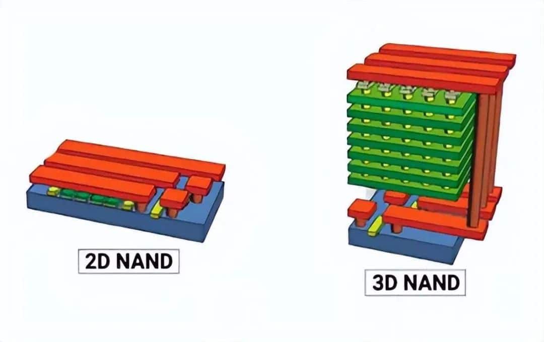
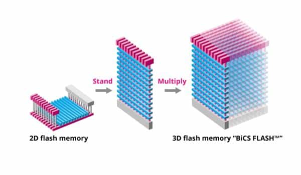
3D NAND stacking is a major development in NAND flash technology, allowing storage capacity to grow without increasing size. This technique helps QLC overcome endurance issues, making it faster, more durable, and reliable while maintaining a low cost.
With continued improvements, QLC will be better equipped for high-demand applications. It will soon compete with TLC and MLC for enterprise storage and gaming.
Looking ahead, NAND flash will aim for more efficiency and reliability at lower costs. As storage needs rise, especially in cloud and data-driven fields, customized solutions will be more common. QLC will likely dominate the consumer market, while TLC and MLC will remain the preferred choice for professionals.

Conclusion

Criteria

QLC

TLC

Cost

More affordable

Slightly more expensive

Endurance

Lower lifespan (fewer P/E cycles)

Better endurance

Speed

Slower, especially with large writes

Faster read/write speeds

Best Use

Budget SSDs, large storage

Performance-focused SSDs for workstations, gaming, etc.

Capacity

Higher storage density

Lower density compared to QLC

In a nutshell, QLC is suitable for those who need budget-friendly storage for everyday use. On the other hand, TLC offers faster speeds, better performance, and high durability for heavy tasks. Choose based on your specific needs.

TLC VS QLC

Which is Better: TLC vs QLC?

TLC vs QLC: A Quick Overview

TLC VS QLC, TLC and QLC are types of NAND flash memory. They store data in cells, with each cell holding multiple bits. The more bits in a cell, the more storage capacity, but can slow down performance and reduce durability.

  • Triple-Level Cell holds 3 bits per cell, balancing capacity, price, and speed. It’s commonly used in SSDs and memory cards for general consumers.
  • Quad-Level Cell stores 4 bits per cell, offering larger storage at a lower price. But, this increased capacity comes with some trade-offs in performance and longevity.

This write-up compares both, showing you which is best for your device—like an SSD, SD card, or laptop upgrade.

Key Differences Between TLC and QLC

TLC and QLC flash storage vary in many ways, from cost to capacity and speed.
QLC VS TLC NAND FLASH

Cost

TLC and QLC NAND flash have a notable cost difference. With QLC storing four bits per cell, it’s generally cheaper than TLC, which only holds three bits. This extra data capacity in QLC lets manufacturers reduce production costs, allowing more storage in the same space.
However, QLC’s lower cost often means reduced speed and durability. For those seeking affordable, high-capacity storage, like for media libraries, QLC can be a solid choice. But, for high-performance or long-lasting storage, QLC’s compromises may not be worth the savings.

TLC VS QLC Lifespan and Durability

With three bits per cell, TLC is more durable than QLC, which holds four. This extra bit in QLC causes cells to wear down faster under frequent use. TLC handles more write-and-erase cycles and performs well under heavy tasks like gaming or workstation applications. QLC, in contrast, is ideal for data that is mostly read and rarely changed.

TLC VS QLC Speed and Performance

TLC tends to outperform QLC in speed and performance. It’s faster because it uses three bits per cell, making data processing quicker with less voltage consumption. This is especially noticeable in tasks like video editing, gaming, and software development, where frequent data writing is required.
TLC’s faster write speeds enhance both efficiency and overall experience. On the other hand, QLC is slower and might not handle demanding tasks well, but it works fine for basic storage like photos or media files.

TLC VS QLC Storage Capacity

QLC drives are great for those who need large storage. With the ability to store four bits per cell, it achieves high density and offers massive storage capacities, often reaching 4TB or more, all at a lower price than comparable TLC drives. This makes QLC a strong contender for archiving and backup needs.

Other Differences to Keep in Mind

  • Power Use: TLC consumes more power because it stores three bits per cell. For most users, the difference isn’t significant.
  • Heat: TLC generally creates less heat because it handles more write cycles without issue. QLC, due to its denser cells, may struggle with heat over time.
  • Endurance and Use: TLC is more durable and works better across various tasks. QLC is ideal for light tasks like storing large files or backups where frequent writes aren’t required.

Relationship Between NAND Flash Types and Memory Cards

The performance of SSDs, SD cards, and microSD cards depends largely on the NAND flash type. SLC, TLC, and QLC each have their unique effects.

MicroSD Cards

  • TLC Flash: More durable and faster, making it ideal for tasks with frequent writes like 4K video recording and high-speed photography. It offers better performance and reliability.
  • QLC Flash: More affordable but slower and less durable. Best for storage-heavy tasks like media backups or long-term storage, but not suitable for high-performance needs.

SSDs

  • TLC Flash: Offers a balance between price and performance, with solid read/write speeds and better durability than QLC. Great for general computing, gaming, and applications.
  • QLC Flash: Cheaper but slower and less durable. Best for more storage needs like data archiving or home servers, but not recommended for high-demand tasks.

SD Cards

  • TLC SD Cards: Best for 4K video or high-resolution images, offering fast write speeds and good durability for professional use.
  • QLC SD Cards: Suitable for basic storage needs, like casual photography or personal use, where speed and frequent writes aren’t crucial.

TLC vs QLC: A Quick Comparison

Best Use Cases for TLC

TLC is ideal for users who need a balance between performance and reliability. It handles fast data access and long-term durability well, making it great for demanding tasks.
For gamers, TLC’s fast read and write speeds ensure smooth gameplay and quick load times. Professionals working on video editing or 3D rendering will find TLC’s ability to manage frequent large data transfers helpful. Content creators can rely on TLC for large, high-resolution files.
While TLC is more expensive than QLC, its consistent performance and durability make it a good investment if you need reliable storage for heavy tasks.

Best Use Cases for QLC

QLC memory caters to users needing substantial storage on a budget. It provides plenty of room but sacrifices speed, making it less ideal for users with high-performance needs.
QLC shines in media storage, offering plenty of room for large files like videos and photos at a lower price. It’s perfect for backups or casual storage needs, where speed isn’t as critical. If you’re doing lighter tasks or just need storage for everyday files, QLC is a solid choice.

Performance Benchmarks

TLC drives typically offer write speeds of around 500–550 MB/s. These speeds make TLC suitable for gaming, video editing, and handling large files easily.
QLC drives are generally slower, with write speeds between 300 and 500 MB/s. While this is slower, it’s fine for everyday tasks like file storage or light editing. However, frequent large file writes could slow things down. For users prioritizing heavy writes or long-term reliability, TLC is better. But for those who need bulk storage on a budget, QLC still delivers.

Future of NAND Flash

As storage demands rise, the NAND flash industry is adapting quickly. QLC (Quad-Level Cell) is gaining traction, with improved speed, durability, and efficiency shaping its future in the consumer market.
One advancement is 3D NAND stacking. This technology increases storage capacity while improving efficiency and lifespan by stacking memory cells vertically. The stacked structure reduces wear on cells during read/write operations, helping extend the life of devices like SSDs and microSD cards.
3D NAND stacking enables QLC to offer larger capacities without compromising performance. Additionally, better wear leveling and error correction algorithms are helping close the gap between QLC and TLC (Triple-Level Cell), making QLC a solid choice for budget-conscious consumers.

Final Words

The right option depends on your needs.

  • Choose TLC for reliable, long-lasting performance and faster speeds for tasks like gaming or video editing.
  • QLC is a good budget option if you need a lot of storage. It’s slower and not as durable, but it’s enough for tasks like archiving or media storage.

Factor

TLC (Triple-Level Cell)

QLC (Quad-Level Cell)

Cost

Higher, but offers better performance and durability.

More affordable, ideal for large storage needs.

Lifespan

Longer lifespan, good for frequent write-heavy tasks.

Shorter lifespan, not ideal for high-write environments.

Speed

Faster read and write speeds, suitable for performance tasks.

Slower performance, better for light read/write use.

Storage Capacity

Lower storage density compared to QLC.

Higher storage density, great for large capacity needs.

Best For

Gaming, video editing, OS drives, and frequent data writes.

Backups, media storage, and light usage.

0
Back to Top
Product has been added to your cart